PCT1789W DATA SHEET
PRELIMINARY
PCT303DW CONTROL REGISTERS
!!
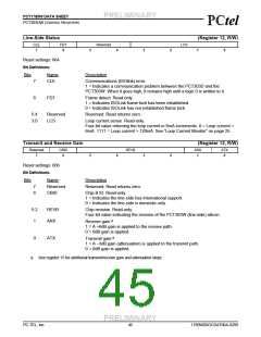
Line-Side Status
(Register 12, R/W)
CLE
FDT
Reserved
LCS
7
6
5
4
3
2
1
0
Reset settings: N/A
Bit Definitions:
Bits
Name
CLE
Description
Communications (ISOlink) error.
1 = Indicates a communication problem between the PCT303D and the
7
6
PCT303W. When it goes high, it remains high until a logic 0 is written to it.
FDT
Frame detect. Read-only.
1 = Indicates ISOLink frame lock has been established.
0 = Indicates ISOLink has not established frame lock.
5:4
3:0
Reserved
LCS
Reserved. Read returns zero.
Loop current sense. Read-only.
Four-bit value returning the loop current in 6mA increments. 0 = Loop current <
6mA. 1111 = Loop current > 120mA. See “Loop Current Monitor” on page 25.
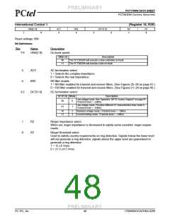
Transmit and Receive Gain
(Register 13, R/W)
Reserved
CBID
REVB
ARX
ATX
7
6
5
4
3
2
1
0
Reset settings: 00h
Bit Definitions:
Bits
Name
Description
7
6
Reserved
CBID
Reserved. Read returns zero.
Chip B ID. Read-only.
1 = Indicates the line-side has international support.
0 = Indicates the line-side is domestic only.
5:2
1
REVB
ARX
Chip revision. Read-only.
Four-bit value indicating the revision of the PCT303W (line-side) silicon.
Receive gain.a
1 = A +6dB gain is applied to the receive path.
0 = 0dB gain is applied.
Transmit gain.a
0
ATX
1 = A –3dB gain (attenuation) is applied to the transmit path.
0 = 0dB gain is applied.
a. See register 15 for additional transmit/receive gain and attenuation steps.
PRELIMINARY
PC-TEL, Inc.
45
1789W0DOCDAT06A-0299

 ETC [ ETC ]