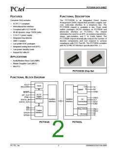
PCT2303N DATA SHEET
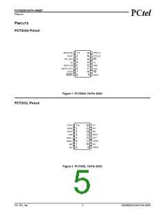
PIN DESCRIPTIONS
!!
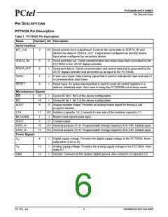
PIN DESCRIPTIONS
PCT303A Pin Description
Table 1 PCT303A Pin Description
Name
Number I/O Description
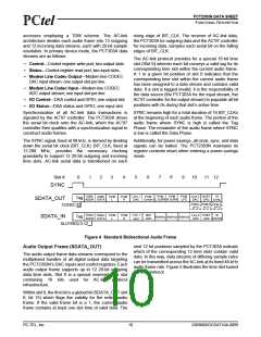
Serial Interface
BIT_CLK
3
I/O Serial port bit clock output/input. Controls the serial data on SDATA_IN and
latches the data on SDATA_OUT. Output when configured as primary device.
Input when configured as secondary device.
SDATA_IN
SDATA_OUT
SYNC
5
6
7
8
O
I
Serial port data out. Serial communication and status data that is provided by the
PCT303A to the AC’97 digital controller.
Serial port data in. Serial communication and control data that is generated by the
AC’97 digital controller and presented as an input to the PCT303A.
I
Frame sync input. Data framing signal that is used to indicate the start and stop of
a communication data frame.
RESET
I
Reset input. An active-low input that is used to reset all control registers to a
defined, initialized state. Also used to bring the PCT2303N out of sleep mode.
Miscellaneous Signals
ID0
10
14
9
I
I
Device ID bit 0. Bit 0 of the device configuration.
Device ID bit 1. Bit 1 of the device configuration.
ID1
AOUT
O
Analog speaker output. Provides an analog output signal for driving a call
progress speaker.
C1A
11
1
I/O Isolation capacitor 1A. Connects to one side of the isolation capacitor C1.
MCLK/XIN
XOUT
I
Master clock input/crystal input.
Crystal output.
2
O
GPIO_A
GPIO_B
Power Signals
VD
16
15
I/O General-purpose I/O A. Programmable through registers 4Ch–54h. Default input.
I/O General-purpose I/O B. Programmable through registers 4Ch–54h. Default input.
4
I
I
I
Digital supply voltage. Provides the digital supply voltage to the PCT303A. Nomi-
nally either 3.3V or 5V.
VA
13
12
Analog supply voltage. Provides the analog supply voltage to the PCT303A. Nom-
inally 5V.
GND
Ground. Connects to the system digital ground. Also connects to capacitor C2.
PC-TEL, Inc.
6
2303N0DOCDAT10A-0899

 ETC [ ETC ]