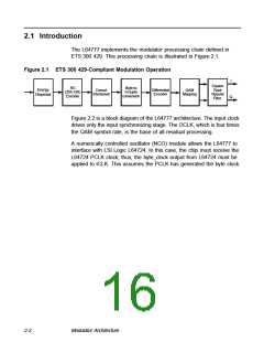
2.1 Introduction
The L64777 implements the modulator processing chain defined in
ETS 300 429. This processing chain is illustrated in Figure 2.1.
Figure 2.1 ETS 300 429-Compliant Modulation Operation
I
Square
Root
Nyquist
Filter
RS
(204,188)
Encoder
Byte to
m-tuple
conversion
Energy
Dispersal
Convol.
Interleaver
Differential
Encoder
QAM
Mapping
Q
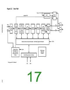
Figure 2.2 is a block diagram of the L64777 architecture. The input clock
drives only the input synchronizing stage. The OCLK, which is four times
the QAM symbol rate, is the base of all residual processing.
A numerically controlled oscillator (NCO) module allows the L64777 to
interface with LSI Logic L64724. In this case, the chip must receive the
L64724 PCLK clock; thus, the byte_clock output from L64724 must be
applied to ICLK. This assumes the PCLK has generated the byte clock.
2-2
Modulator Architecture

 ETC [ ETC ]