Functional Description
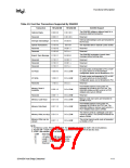
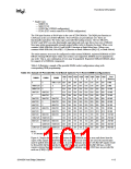
Table 4-7. Host Special Cycles with 82443BX
Special
BE[7:0}#
Action Taken
Cycle Type
This transaction is issued when an agent has completed a cache sync and flush
operation in response to an earlier FLUSH# signal assertion. The 82443BX
claims this cycle and retires it.
0000
0101
Flush
Acknowledge
This transaction is issued when an agent enters Stop Clock mode. This cycle is
claimed by the 82443BX and propagated to the PCI as a Special Stop Grant
Acknowledge Cycle. This cycle is completed on the CPU bus after it is terminated on the PCI
via a master abort mechanism.
0000
0110
Stop Clock
0000
0111
SMI
This transaction is first issued when an agent enters the System Management
Acknowledge Mode (SMM).
all others
Reserved
NOTE:
1. None of the host bus special cycles is propagated to the AGP interface.
4.2.2
Symmetric Multiprocessor (SMP) Protocol Support
The Intel® 440BX AGPset is optimized for uniprocessor system and also supports the symmetrical
multiprocessor configurations of up to two CPUs on the host bus.
When configured for dual-processor, the Intel® 440BX AGPset-based platform must integrate an
I/O APIC functionality and WSC# signaling mechanism must be enabled.
4.2.3
4.2.4
In-Order Queue Pipelining
The 82443BX interface to the CPU bus includes a four deep in-order queue to track pipelined bus
transactions.
Frame Buffer Memory Support (USWC)
To allow for high speed write capability for graphics, the Pentium Pro processor family has
introduced USWC memory type. The USWC (uncacheable, speculative, write-combining) memory
type provides a write-combining buffering mechanism for write operations. A high percentage of
graphics transactions are writes to the memory-mapped graphics region, normally known as the
linear frame buffer. Reads and writes to USWC are non-cached and can have no side effects.
In the case of graphics, current 32-bit drivers (without modifications) would use Partial Write
protocol to update the frame buffer. The highest performance write transaction on the CPU bus is
the Line Write.
82443BX Host Bridge Datasheet
4-13

 ETC [ ETC ]