Functional Description
• Single Copy
— MD[63:0]
— MECC[7:0]
— GCKE (for 4 DIMM configuration)
— FENA (FET switch control for 4 DIMM configuration)
The CS# pins function as RAS# pins in the case of EDO DRAMs. The DQM pins function as
CAS# pins in the case of EDO DRAMs. Two CS# lines are provided per row. These are
functionally equivalent. The extra copy is provided for loading reasons. The two SRAS#’s,
SCAS#’s and WE#’s are also functionally equivalent and each copy drives two rows of DRAM.
Most pins utilize programmable strength output buffers (refer to Register Section). When a row
contains 16Mb SDRAMs, MAA11 and MAB11 function as Bank Select lines. When a row
contains 64Mb SDRAMs, MAA/B[12:11] function as Bank Addresses (BA[1:0], or Bank Selects).
The entire memory array may be configured as either normal SDRAM, registered SDRAM or EDO
DRAM. Mixing DRAM types within one system is not supported. DIMMs may be populated in
any order. That is, any combination of rows may be populated. Registered SDRAM DIMMs allow
for support of x4 SDRAM components.
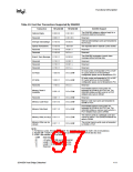
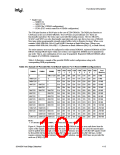
Table 4-8 illustrates a sample of the possible DIMM socket configurations along with
corresponding DRB programming.
Table 4-8. Sample Of Possible Mix And Match Options For 6 Row/3 DIMM Configurations
DRB DRB DRB DRB DRB DRB DRB DRB
Total
Memory
DIMM0\
DIMM1
DIMM2
0
1
2
3
4
5
6
7
0
0
0
0
1MB x 72/S 00h
00h
01h
02h
01h
00h
02h
04h
04h
04h
08h
08h
10h
08h
00h
20h
00h
01h
02h
02h
04h
03h
04h
04h
08h
08h
00h
01h
02h
02h
04h
04h
04h
04h
08h
08h
01h
01h
02h
02h
04h
05h
05h
08h
09h
01h
01h
02h
02h
04h
06h
06h
08h
10h
01h
01h
02h
02h
04h
06h
06h
08h
10h
01h
01h
02h
02h
04h
06h
06h
08h
10h
8 MB
1MBx72/S
2MBx72/S
1Mx72/S
0
0
01h
02h
01h
00h
01h
04h
04h
04h
04h
04h
10h
04h
00h
10h
8 MB
0
16 MB
16 MB
32 MB
48 MB
48 MB
64 MB
80 MB
96 MB
192 MB
256 MB
256 MB
384 MB
640 MB
1Mx72/S
4Mx72/S
2Mx72/D
0
0
0
2Mx72/D
4Mx72/S
4Mx72/S
4Mx72/S
8Mx72/D
8Mx72/D
2Mx72/D
2Mx72/D
4Mx72/S
2Mx72/D
4Mx72/S
8Mx72/D
0
0
4Mx72/S
0
0Ch 0Ch 0Ch 0Ch
8Mx72/D
0Ch 10h
14h
20h
18h
20h
18h
20h
20h
30h
50h
18h
20h
20h
30h
50h
16Mx72/S 16Mx72/S
20h
18h
10h
30h
20h
18h
20h
40h
8Mx72/D
0
16Mx72/S 8Mx72/D
32Mx72/D 16Mx72/S
1Ch 20h
30h
50h
30h
50h
32Mx72/D 32Mx72/D 16Mx72/S
NOTE:
1. "S" denotes single-sided DIMM's, "D" denotes double-sided DIMM's.
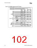
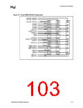
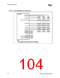
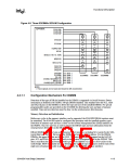
Figure 4-2 depicts the 82443BX connections for an SDRAM memory array and shows how the
copies of the signals are distributed to the array. If cross bar switches are used, the unused input
must be pulled down through a resistor. In an EDO memory array, the CSA/B[5:0]# signals would
be RASA/B[5:0]# lines and the DQMA/B[7:0] signals would be CASA/B[7:0]# lines. GCKE
requires external logic (not shown). For a 3 DIMM solution, separate CKE lines are provided for
each row (CKE[5:0]).
82443BX Host Bridge Datasheet
4-15

 ETC [ ETC ]