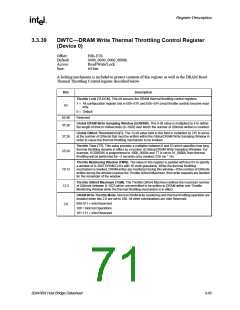
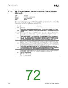
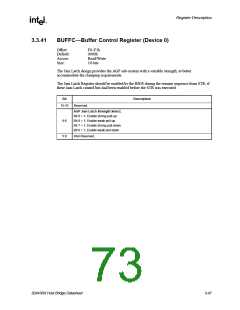
Register Description
Bit
Description
DQMB1/CASB1# (100 MHz/66 MHz buffer select bit). This bit enables either 100 MHz or 66
MHz buffers for DQMB1/CASB1#.
3
2
0 = 66 MHz
1 = 100 MHz
DQMA[7:6,4:2,0]/CASA[7:6,4:2,0]# (100 MHz/66 MHz buffer select bit). This bit enables
either 100 MHz or 66 MHz buffers for DQMA[7:6]/CASA[7:6]#, DQMA[4:2]/CASA[4:2]#, and the
DQMA[0]/CASA[0]#.
0 = 66 MHz
1 = 100 MHz
CKE1/GCKE (100 MHz/66 MHz buffer select bit). This bit enables either 100 MHz or 66 MHz
buffers forCKE1.
1
0
0 = 66 MHz
1 = 100 MHz
CKE0/FENA (100 MHz/66 MHz buffer select bit). This bit enables either 100 MHz or 66 MHz
buffers for CKE0/FENA.
0 = 66 MHz
1 = 100 MHz
3.3.38
BSPAD—BIOS Scratch Pad Register (Device 0)
Address Offset:
Default Value:
Access:
D0–D7h
0000-0000-0000-0000h
Read/Write
64 bits
Size:
This register provides 8 bytes general purpose read/write registers for the BIOS to perform the
configuration routine. The 82443BX will provide this 8 byte register in the PCI configuration space
of the 82443BX device0 on bus 0. The registers in this range will be defined as read/write and will
be initialized to all 0’s after PCIRST#. The BIOS will can access these registers through the normal
PCI configuration register mechanism, accessing 1,2 or 4 bytes in every data access.
Bit
Description
64:0
BIOS Work Space.
3-44
82443BX Host Bridge Datasheet

 ETC [ ETC ]