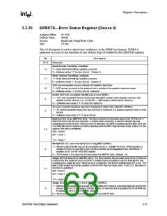
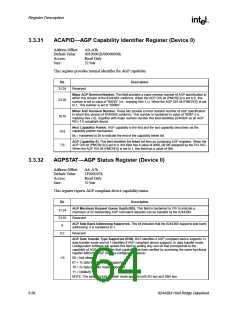
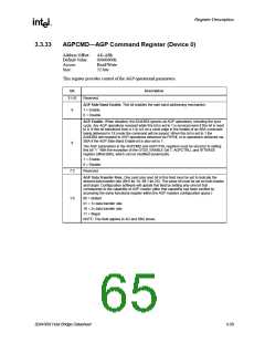
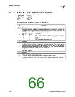
Register Description
3.3.35
APSIZE—Aperture Size Register (Device 0)
Address Offset:
Default Value:
Access:
B4h
00h
Read/Write
8 bits
Size:
This register determines the effective size of the Graphics Aperture used for a particular 82443BX
configuration. This register can be updated by the 82443BX-specific BIOS configuration sequence
before the PCI normal bus enumeration sequence takes place. If the register is not updated, a
default value selects an aperture of maximum size (i.e., 256 MB). The size of the table that will
correspond to a 256 MB aperture is not practical for most applications and, therefore, these bits
must be programmed to a smaller practical value that forces adequate address range to be requested
via the APBASE register from the PCI configuration software.
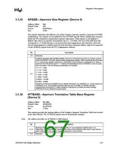
Bit
Description
7:6
Reserved.
Graphics Aperture Size (APSIZE) (R/W). Each bit in APSIZE[5:0] operates on similarly ordered
bits in APBASE[27:22] of the Aperture Base configuration register. When a particular bit of this field
is “0”, it forces the similarly ordered bit in APBASE[27:22] to behave as “hardwired” to 0. When a
particular bit of this field is set to “1”, it allows corresponding bit of the APBASE[27:22] to be read/
write accessible. Only the following combinations are allowed:
11 1111 = 4 MB
11 1110 = 8 MB
11 1100 = 16 MB
11 1000 = 32 MB
11 0000 = 64 MB
10 0000 = 128 MB
00 0000 = 256MB
5:0
Default for APSIZE[5:0]=000000b forces default APBASE[27:22] =000000b (i.e., all bits respond as
“hardwired” to 0). This provides maximum aperture size of 256 MB. As another example,
programming APSIZE[5:0]=111000b hardwires APBASE[24:22]=000b and while enabling
APBASE[27:25] as read/write programmable.
3.3.36
ATTBASE—Aperture Translation Table Base Register
(Device 0)
Address Offset:
Default Value:
Access:
B8–BBh
00000000h
Read/Write
32 bits
Size:
This register provides the starting address of the Graphics Aperture Translation Table base located
in the main DRAM. The ATTBASE register may be dynamically changed.
Note: The address provided via ATTBASE is 4KB aligned.
Bit
Description
Aperture Translation Table Base Address. Bits 31:12 correspond to address bits 31:12,
respectively. This field contains a pointer to the base of the translation table used to map memory
space addresses in the aperture range to addresses in main memory.
31:12
11:0
Reserved.
82443BX Host Bridge Datasheet
3-41

 ETC [ ETC ]