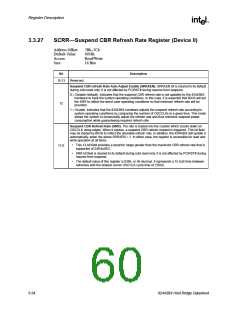
Register Description
Bit
Description
SDRAM Mode Select (SMS). These bits allow the 82443BX to drive various commands to the
SDRAMs. These special modes are intended for initialization at power up.
SMS
000
001
Mode
Normal SDRAM Operation. (default)
NOP Command Enable. In this mode all CPU cycles to SDRAM result in NOP
Command on the SDRAM interface.
010
011
All Banks Precharge Enable. In this mode all CPU cycles to SDRAM result in an All
Banks Precharge Command on the SDRAM interface.
Mode Register Set Enable. In this mode all CPU cycles to SDRAM result in a mode
register set command on the SDRAM interface. The Command is driven on the
MAx[13:0] lines. MAx[2:0] must always be driven to 010 for burst of 4 mode. MA3 must
be driven to 1 for interleave wrap type. MAx4 needs to be driven to the value
programmed in the CAS# Latency bit. MAx[6:5] should always be driven to 01.
MAx[12:7] must be driven to 000000. BIOS must calculate and drive the correct host
address for each row of memory such that the correct command is driven on the
MAx[12:0] lines.
7:5
100
CBR Enable. In this mode all CPU cycles to SDRAM result in a CBR cycle on the
SDRAM interface.
101
110
111
Reserved.
Reserved.
Reserved.
Note: BIOS must take into consideration MAB inversion when programming for 3 and 4 DIMM.
SDRAMPWR. The SDRAMPWR bit controls how the CKE signals are driven for different DRAM
configurations. For a 3 DIMM configuration, SDRAMPWR should be set to ‘0’. For a 4 DIMM
configuration, SDRAMPWR should be set to ‘1’. In this case the 82443BX drives a single CKE
signal (GCKE). The combination of SDRAMPWR and MMCONFIG (DRAMC register) determine
the functioning of the CKE signals. Refer to the DRAMC register (Section 3.3.15, “DRAMC—
DRAM Control Register (Device 0)” on page 3-19) for more details.
4
Note: When PCIRST# assertion occurs during POS/STR, these bits are not reset to 0.
Leadoff Command Timing (LCT). These bits control when the SDRAM command pins
(SRASx#, SCASx# and WEx#) and CSx# are considered valid on leadoffs for CPU cycles.
0 = 4 CS# Clock
1 = 3 CS# Clock
The LCT Bit should be initialized by BIOS as recommended below:
3
•
•
Desktop platforms running at 100 MHz should leave the LCT bit set to its default value of 0.
Desktop platforms running at 66 MHz should leave the LCT bit set to its default value of 0, if
load on either MAA or MAB signals is > 9. Otherwise, set the LCT bit to 1, if load on both
MAA and MAB is ≤ 9.
•
Mobile platforms will be run at 66MHz and should set the LCT bit to 1.
CAS# Latency (CL). This bit controls the number of CLKs between when a read command is
sampled by the SDRAMs and when the 82443BX samples read data from the SDRAMs. If a
given row is populated with a registered SDRAM DIMM, an extra clock is inserted between the
read command the when the 82443BX samples read data. For a registered DIMM with CL=2,
this bit should be set to 1.
2
0 = 3 DCLK CAS# latency.
1 = 2 DCLK CAS# latency.
SDRAM RAS# to CAS# Delay (SRCD). This bit controls the number of DCLKs from a Row
Activate command to a read or write command.
1
0
0 = 3 clocks will be inserted between a row activate command and either a read or write
command.
1 = 2 clocks will be inserted between a row activate and either a read or write command.
SDRAM RAS# Precharge (SRP). This bit controls the number of DCLKs for RAS# precharge.
0 = 3 clocks of RAS# precharge.
1 = 2 clocks of RAS# precharge.
82443BX Host Bridge Datasheet
3-31

 ETC [ ETC ]