Register Description
3.3.3
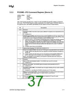
PCICMD—PCI Command Register (Device 0)
Address Offset:
Default:
Access:
04–05h
0006h
Read/Write
16 bits
Size
This 16-bit register provides basic control over the 82443BX PCI interface ability to respond to
PCI cycles. The PCICMD Register enables and disables the SERR# signal, 82443BX response to
PCI special cycles, and enables and disables PCI bus master accesses to main memory.
Bit
Descriptions
15:10
Reserved.
Fast Back-to-Back. Fast back-to-back cycles to different PCI targets are not implemented by the
82443BX.
9
8
0 = Hardwired to 0.
SERR# Enable (SERRE). Note that this bit only controls SERR# for the PCI bus. Device #1 has
its own SERRE bit to control error reporting for the bus conditions occurred on the AGP bus. Two
control bits are used in a logical OR manner to control SERR# pin driver.
1 = If this bit is set to a 1, the 82443BX’s SERR# signal driver is enabled and SERR# is asserted
when an error condition occurs, and the corresponding bit is enabled in the ERRCMD
register. The error status is reported in the ERRSTS and PCISTS registers. Also, if this bit is
set and the 82443BX’s PCI parity error reporting is enabled by the PERRE bit located in this
register, then the 82443BX will report address and data parity errors (when it is potential
target).
0 = SERR# is never driven by the 82443BX.
7
6
Address/Data Stepping. Not implemented (hardwired to 0).
Parity Error Enable (PERRE). Note that the PERR# signal is not implemented by the 82443BX.
1 = Enable. Address and data parity errors are reported via SERR# mechanism (if enabled via
SERRE bit).
0 = Disable. Address and data parity errors are not reported via the 82443BX SERR# signal.
(NOTE: Other types of error conditions can be still signaled via SERR# mechanism.)
NOTE: The 82443BX PCI bus interface is still required to generate parity even if parity error
reporting is disabled via this bit.
5
4
Reserved.
Memory Write and Invalidate Enable. The 82443BX never uses this command.
0 = Hardwired to 0.
Special Cycle Enable. The 82443BX ignores all special cycles generated on the PCI.
3
2
0 = Hardwired to 0.
Bus Master Enable (BME). The 82443BX does not support disabling of its bus master capability
on the PCI Bus.
1 = Hardwired to 1, permitting the 82443BX to function as a PCI Bus master.
Memory Access Enable (MAE). This bit enables/disables PCI master access to main memory
(DRAM). The 82443BX always allows PCI master access to main memory.
1
0
1 = Hardwired to 1.
I/O Access Enable (IOAE). The 82443BX does not respond to PCI bus I/O cycles.
0 = Hardwired to 0.
82443BX Host Bridge Datasheet
3-11

 ETC [ ETC ]