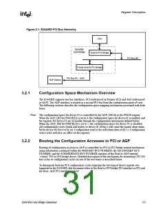
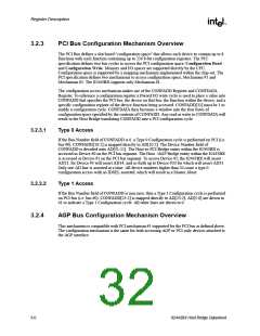
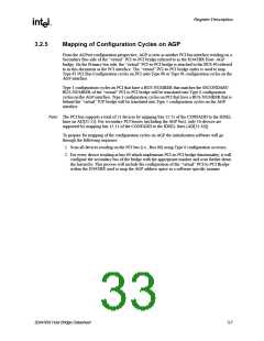
Register Description
3.3
Host-to-PCI Bridge Registers (Device 0)
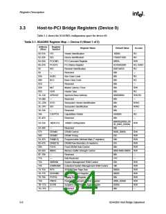
Table 3-1 shows the 82443BX configuration space for device #0.
Table 3-1. 82443BX Register Map — Device 0 (Sheet 1 of 2)
Address
Offset
Register
Symbol
Register Name
Default Value
8086h
Access
RO
00–01h
02–03h
04–05h
06–07h
08
VID
Vendor Identification
DID
Device Identification
PCI Command Register
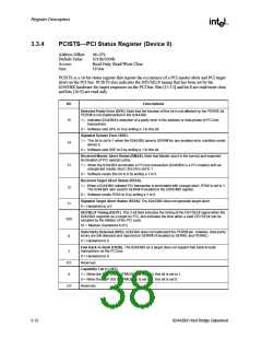
PCI Status Register
Revision Identification
Reserved
7190h/7192h
0006h
0210h/0200h
00/01h/02h
00h
RO
PCICMD
PCISTS
RID
R/W
RO, R/WC
RO
09
—
—
0Ah
SUBC
BCC
—
Sub-Class Code
Base Class Code
Reserved
00h
RO
0Bh
06h
RO
0Ch
00h
—
0Dh
MLT
Master Latency Timer
Header Type
00h
R/W
RO
0Eh
HDR
APBASE
—
00h
10–13h
14–2Bh
2C–2Dh
2E–2Fh
30–33h
34h
Aperture Base Address
Reserved
00000008h
00h
R/W,RO
—
SVID
SID
Subsystem Vendor Identification
Subsystem Identification
Reserved
00h
R/WO
R/WO
—
00h
—
00h
CAPPTR
—
Capabilities Pointer
Reserved
A0h/00h
00h
RO
35–4Fh
—
[0000h]:[00S0_00
00_000S_0S00b]
50–53h
NBXCFG
440BX Configuration
R/W
54–56h
57h
—
Reserved
00h
—
DRAMC
DRAMT
PAM[6:0]
DRB[7:0]
FDHC
MBSC
—
DRAM Control
00S0_0000b
03h
R/W
R/W
R/W
R/W
R/W
58h
DRAM Timing
59–5Fh
60–67h
68h
Programmable Attribute Map (7 registers)
DRAM Row Boundary (8 registers)
Fixed DRAM Hole Control
Memory Buffer Strength Control
Reserved
00h
01h
00h
69–6Eh
6F–70h
71h
0000-0000-0000h R/W
00h
—
—
Intel Reserved
1Fh
—
72h
SMRAM
ESMRAMC
RPS
System Management RAM Control
Extended System Management RAM Control.
SDRAM Row Page Size
SDRAM Control Register
Paging Policy Register
02h
R/W
R/W
R/W
R/W
R/W
R/W
R/W
—
73h
38h
74–75h
76–77h
78–79h
7Ah
0000h
0000h
00h
SDRAMC
PGPOL
PMCR
SCRR
—
Power Management Control Register
Suspend CBR Refresh Rate Register
Reserved
0000_S0S0b
0038h
00h
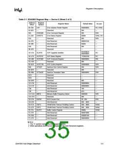
7B–7Ch
7D–7Fh
3-8
82443BX Host Bridge Datasheet

 ETC [ ETC ]