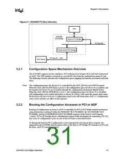
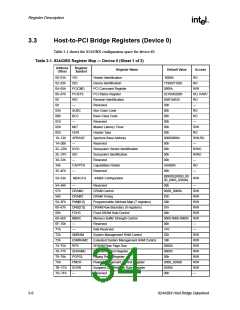
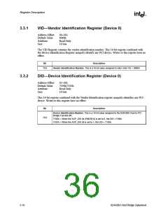
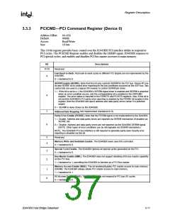
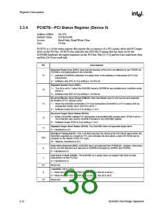
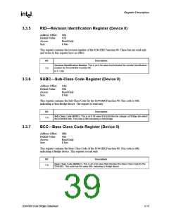
Register Description
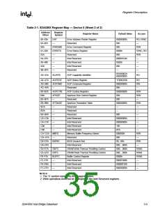
Table 3-1. 82443BX Register Map — Device 0 (Sheet 2 of 2)
Address
Offset
Register
Symbol
Register Name
Default Value
Access
80–83h
84–8Fh
90h
EAP
Error Address Pointer Register
Reserved
00000000h
00h
RO, R/WC
—
—
ERRCMD
Error Command Register
Error Status Register
Reserved
80h
R/W
91–92h
93h
ERRSTS
0000h
00h
R/WC, RO
—
—
—
—
—
R/W
—
94–97h
98–99h
9Ah
Intel Reserved
00006104h
0500h
00h
Intel Reserved
—
Intel Reserved
—
9B–9Fh
Reserved
—
—
00100002h
00000000h
A0–A3h
ACAPID
AGP Capability Identifier
RO
A4–A7h
A8–ABh
AC–AFh
B0–B3h
B4h
AGPSTAT
AGP Status Register
AGP Command Register
Reserved
1F000203h
00000000h
00h
RO
RW
—
AGPCMD
—
AGPCTRL
AGP Control Register)
Aperture Size Control Register
Reserved
00000000h
00h
R/W
R/W
—
APSIZE
B5–B7h
B8–BBh
BCh
—
00h
ATTBASE
Aperture Translation Table
Reserved
00000000h
—
R/W
—
—
—
—
—
—
—
—
BDh
Reserved
—
—
BE–BFh
C0–C3h
C4–C7h
C8h
Reserved
00h
—
Intel Reserved
00000000h
00000000h
18h
—
Intel Reserved
—
Intel Reserved
—
C9h
Intel Reserved
0Ch
—
CA–CCh MBFS
Memory Buffer Frequency Select
Reserved
000000h
00h
R/W
—
CD–CFh
D0–D7h
D8–DFh
E0–E7h
E8–EFh
F0–F1h
F2–F7h
F8–FBh
FC–FFh
—
BSPAD
BIOS Scratch Pad
Intel Reserved
00...00h
000....000h
000....000h
000....000h
0000h
R/W
—
DWTC
DRTC
BUFFC
—
DRAM Write Thermal Throttling Control
DRAM Read Thermal Throttling Control
Buffer Control Register
Intel Reserved
R/W/L
R/W/L
R/W/L
—
0000F800h
00000F20h
00000000h
—
Intel Reserved
—
—
Intel Reserved
—
NOTES:
1. The ‘S’ symbol represents the strapping option.
2. Write operations must not be attempted to the Intel Reserved registers.
82443BX Host Bridge Datasheet
3-9

 ETC [ ETC ]