NT5DS32M4AT
NT5DS16M8AT
128Mb Double Data Rate SDRAM
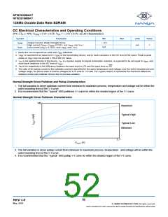
DC Electrical Characteristics and Operating Conditions
(0°C £ TA £ 70°C; VDDQ = 2.5V ± 0.2V, VDD = + 2.5V ± 0.2V, see AC Characteristics)
Symbol
Parameter
Min
- 9.0
9.0
Max
Units
mA
Notes
1
I
I
Output Current: Weak Strength Driver
OHW
OLW
High current (V
Low current (V
= V
-0.763V, min V
, min V
)
TT
OUT
DDQ
REF
= 0.763V, max V
, max V
REF
)
OUT
TT
1. Inputs are not recognized as valid until V
stabilizes.
REF
2.
V
is expected to be equal to 0.5 V
of the transmitting device, and to track variations in the DC level of the same. Peak-to-peak
DDQ
REF
noise on V
may not exceed ± 2% of the DC value.
REF
3.
4.
V
is not applied directly to the device. V is a system supply for signal termination resistors, is expected to be set equal to V
, and
TT
TT
REF
must track variations in the DC level of V
.
REF
V
is the magnitude of the difference between the input level on CK and the input level on CK
ID
5. The ratio of the pullup current to the pulldown current is specified for the same temperature and voltage, over the entire tempera-ture and
voltage range, for device drain to source voltages for 0.25 volts to 1.0 volts. For a given output, it represents the maximum difference
between pullup and pulldown drivers due to process variation.
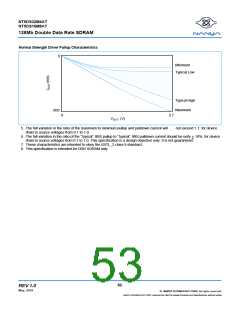
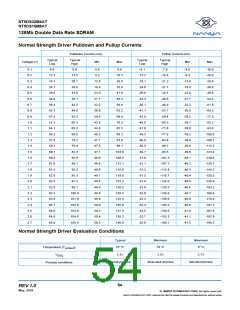
Normal Strength Driver Pulldown and Pullup Characteristics
1. The full variation in driver pulldown current from minimum to maximum process, temperature and voltage will lie within the
outer bounding lines of the V-I curve.
2. It is recommended that the “typical” IBIS pulldown V-I curve lie within the shaded region of the V-I curve.
Normal Strength Driver Pulldown Characteristics
140
Maximum
Typical High
Typical Low
Minimum
0
0
2.7
VOUT (V)
3. The full variation in driver pullup current from minimum to maximum process, temperature and voltage will lie within the
outer bounding lines of the V-I curve.
4. It is recommended that the “typical” IBIS pullup V-I curve lie within the shaded region of the V-I curve.
52
REV 1.0
May, 2001
©
NANYA TECHNOLOGY CORP. All rights reserved.
NANYA TECHNOLOGY CORP. reserves the right to change Products and Specifications without notice.

 ETC [ ETC ]