AC Characteristics
TCASE = -40 °C to +95 °C, appropriate heat sinking may be required, for package parts. Device is AC-tested in the temperature
range 0 °C to 85 °C, specifications from -40 °C to +95 °C are guaranteed by design.
TDIE BACK = -30 °C to +100 °C, appropriate heat sinking may be required, for dies. Die is not AC-tested. Specifications are
guaranteed by design.
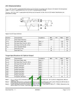
Figure 12.LDD Output Definition.
Symbol:
Characteristic:
Conditions:
MIN.:
TYP.:
MAX.:
UNIT:
Mbit/s
UIPP
ps
fMAX OUT
Data Output Frequency
IM Output Pattern Jitter
IM Output Rise Time (20 - 80 %)
IM Output Fall Time (80 - 20 %)
Duty Adjustable Range
Data Set-up Time
2500
J
pp IM
Note 1, 2
Note 1
0.06
100
100
+20
t
t
RISE IM
FALL IM
Note 1
ps
Drange
tS
0
%
60
60
ps
tH
Data Hold Time
ps
Target Specifications for Optical Output
Symbol:
Characteristic:
Conditions:
Note 3, 2
Note 3
MIN.:
TYP.:
MAX.:
0.06
100
100
-
UNIT:
UIPP
ps
ps
%
J
pp IM
IM Output Pattern Jitter
IM Output Rise Time (20 - 80 %)
IM Output Fall Time (80 - 20 %)
Ringing, See figure
t
t
RISE IM
FALL IM
Note 3
h1/H
h2/H
h3/H
h4/H
h5/H
h6/H
hx/H
Note 3
Ringing, See figure
Note 3
12
7
%
Ringing, See figure
Note 3
%
Ringing, See figure
Note 3
7
%
Ringing, See figure
Note 3
15
-
%
Ringing, See figure
Note 3
%
Crosspoint, See figure
Note 3
45
55
%
Note 1: RLOAD = 25 W to VCC connected to pin IM. ILD = 50 mA. Rise/Fall times at 20 – 80 % of HI/LO voltage levels. IMB con-
nected to VCC.
Note 2: Added jitter. Measured as a peak-peak jitter value on a sampling oscilloscope in 60 s period. Measured with the data re-
timing enabled, and using the retiming clock signal as trigger for the oscilloscope.
Note 3: Load is equivalent circuit of LD module, see Figure 10 on page 5 . Input signal is PN23 (223 -1 PRBS). Measured on the
optical output of LD module. These specs are target specs.
Data Sheet Rev.: 11
GD16521
Page 11 of 13

 ETC [ ETC ]