<ꢀ5ꢁꢀꢂꢃ<ꢀ.ꢁꢀꢂ
'PJCPEGFꢄ<ꢁꢀꢂꢄ/KETQRTQEGUUQT
ZiLOG
#4%*+6'%674'
The Z180 combines a high-performance CPU core with a
variety of system and I/O resources useful in a broad range
of applications. The CPU core consists of five functional
blocks: clock generator, bus state controller, Interrupt con-
troller, memory management unit (MMU), and the central
processing unit (CPU). The integrated I/O resources make
up the remaining four functional blocks: direct memory ac-
cess(DMA) control (2 channels), asynchronousserial com-
munication interface (ASCI, 2 channels) programmable re-
load timers (PRT, 2 channels), and a clock serial I/O
(CSI/O) channel.
code maintains compatibility with the Z80 CPU, while of-
fering access to an extended memory space. Accomplished
by using an effective common-area/banked-area scheme.
%GPVTCNꢄ2TQEGUUKPIꢄ7PKVꢆꢄThe CPU is microcoded to pro-
vide a core that is object-code compatible with the Z80
CPU. It also provides a superset of the Z80 instruction set,
including8-bitmultiplication. Thecore ismodifiedtoallow
many of the instructions to execute in fewer clock cycles.
&/#ꢄ%QPVTQNNGTꢆꢄThe DMA controller provides high-
speed transfers between memory and I/O devices. Transfer
operations supported are memory-to-memory, memory
to/from I/O, and I/O-to-I/O. Transfer modes supported are
request, burst, and cycle steal. DMA transfers can access
thefull1-MBaddressrangewithablocklengthupto64 KB,
and can cross over 64K boundaries.
%NQEMꢄ)GPGTCVQTꢆꢄThislogic generatesa system clock from
an external crystal or clock input. The external clock is di-
vided by 2 or 1 and provides the timing for both internal
and external devices.
$WUꢄ5VCVGꢄ%QPVTQNNGTꢆꢄThis logic performs all of the status
and bus-control activity associated with the CPU and some
on-chip peripherals. Also includes wait-state timing, reset
cycles, DRAM refresh, and DMA bus exchanges.
#U[PEJTQPQWUꢄ5GTKCNꢄ%QOOWPKECVKQPꢄ+PVGTHCEGꢄꢌ#5%+ꢍꢆ
The ASCI logic provides two individual full-duplex
UARTs. Each channel includes a programmable baud rate
generator and modem control signals. The ASCI channels
can also support a multiprocessor communication format as
well as break detection and generation
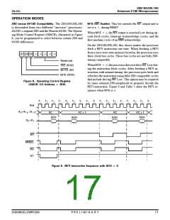
+PVGTTWRVꢄ%QPVTQNNGTꢆꢄThis logic monitors and prioritizes
the variety of internal and external interrupts and traps to
provide the correct responses from the CPU. To maintain
compatibility with the Z80 CPU, three different interrupts
modes are supported.
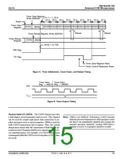
2TQITCOOCDNGꢄ4GNQCFꢄ6KOGTUꢄꢌ246ꢍꢆꢄThis logic consists
of two separate channels, each containing a 16-bit counter
(timer) and count reload register. The time base for the
counters is derived from the system clock (divided by 20)
before reaching the counter. PRT channel 1 provides an op-
tional output to allow for waveform generation.
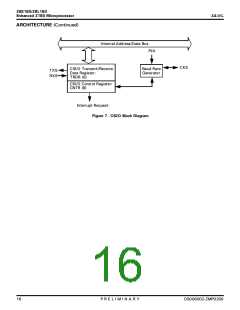
/GOQT[ꢄ/CPCIGOGPVꢄ7PKVꢆꢄThe MMU allows the user to
map the memory used by the CPU (logically only 64KB)
into the 1-MB addressing range supported by the
Z8S180/Z8L180. The organization of the MMU object
ꢄꢎ
2ꢅ4ꢅ'ꢅ.ꢅ+ꢅ/ꢅ+ꢅ0ꢅ#ꢅ4ꢅ;
&5ꢀꢀꢁꢀꢀꢂꢃ</2ꢀꢂꢀꢀ

 ZILOG [ ZILOG, INC. ]