MVTX2801
Data Sheet
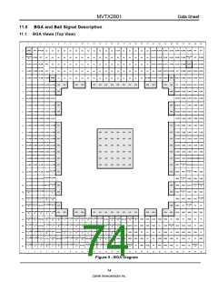
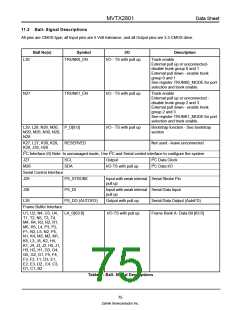
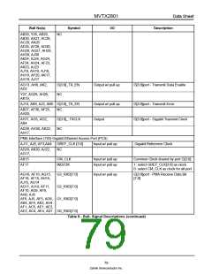
11.2 Ball- Signal Descriptions
All pins are CMOS type; all Input pins are 5 Volt tolerance, and all Output pins are 3.3 CMOS drive.
Ball No(s)
Symbol
I/O
Description
Trunk enable
L30
TRUNK0_EN
I/O - TS with pull up
External pull up or unconnected-
disable trunk group 0 and 1
External pull down - enable trunk
group 0 and 1
See register TRUNK0_MODE for port
selection and trunk enable.
N27
TRUNK1_EN
I/O - TS with pull up
Trunk enable
External pull up or unconnected -
disable trunk group 2 and 3
External pull down - enable trunk
group 2 and 3
See register TRUNK1_MODE for port
selection and trunk enable.
L29, L28, N26, M30, P_D[8:0]
M29, M28, N30, N29,
N28
I/O - TS with pull up
Bootstrap function - See bootstrap
section
K27, L27, K30, K29,
RESERVED
Not used - leave unconnected
K28, J28, H28
2
2
I C Interface (0) Note: In unmanaged mode, Use I C and Serial control interface to configure the system
2
J27
M26
SCL
SDA
Output
I/O-TS with pull up
I C Data Clock
2
I C Data I/O
Serial Control Interface
J29
PS_STROBE
PS_DI
Input with weak internal Serial Strobe Pin
pull up
J30
Input with weak internal Serial Data Input
pull up
L26
PS_DO (AUTOFD)
Output with pull up
I/O-TS with pull up
Serial Data Output (AutoFD)
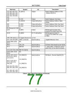
Frame Bank A- Data Bit [63:0]
Frame Buffer Interface
U1, U2, N4, U3, U4,
T1, T2, N5, T3, T4,
M4, R4, R3, R2, R1,
M5, R5, L4, P3, P2,
P1, N3, L5, N2, P5,
N1, K4, M3, M2, M1,
K5, L3, J5, K2, H4,
K1, J4, J3, J2, H5, J1,
H3, H2, H1, G3, G4,
G5, G2, G1, F5, F4,
F3, F2, F1, D3, E1,
E2, E3, D2., E4, C3,
D1, C1, B2
LA_D[63:0]
Table 8 - Ball- Signal Descriptions
75
Zarlink Semiconductor Inc.

 ZARLINK [ ZARLINK SEMICONDUCTOR INC ]