MVTX2801
Data Sheet
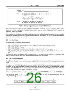
LE_SYNCO
LE_DO
P0
P1
P2
P3
P4
P5
P6
P7
U0
U1
U2
U3
U4
U5
U6
U7
info info info info info info info info
0
1
2
3
4
5
6
7
FC
TxD
RxD
LNK
SP0
SP1
FDX
COL
LE_CLKO
Table 6 - Timing diagram for serial mode in LED interface
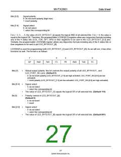
The status bits shown in here are flow control (FC), transmitting data (TxD), receiving data (RxD), link up (LNK),
speed (SP0 and SP1), full duplex (FDX), and collision (COL). Note that SP[1:0] is defined as 10 for 1 Gbps, 01 for
100 Mbps, and 00 for 10 Mbps.
Also note that U0-U7 represent user-defined sub-frames in which additional status information may be embedded.
We will see later that the MVTX2801 provides registers that can be written by the CPU to indicate this additional
status information as it becomes available.
9.3 Parallel Mode
In parallel mode, the following pins are utilized:
•
•
•
•
LED_PORT_SEL[3:0] - indicates which of the 4 Gigabit port status bytes is being read out
LED_PORT_SEL[7:4] - No use.
LED_PORT_SEL[9:8] - indicates which of the 2 user-defined status bytes is being read out
LED_BYTEOUT_[7:0] - provides 8 bits for 4 different port status indicators. Note that these bits are active
low.
By default, the system is in parallel mode. In parallel mode, the 10 status bytes are scanned in a continuous loop,
with one byte read out per clock cycle, and the appropriate port select bit asserted.
9.4 LED Control Registers
An LED Control Register can be used for programming the LED clock rate, sample hold time, and pattern in parallel
mode.
In addition, the MVTX2801 provides 8 registers called LEDUSER[7:0] for user-defined status bytes. During
operation, the CPU can write values to these registers, which will be read out to the LED interface output (serial or
parallel). Only LEDUSER[1:0] are used in parallel mode. The content of the LEDUSER registers will be sent out by
the LED serial shift logic, or in parallel mode, a byte at a time.
Because in parallel mode there are only two user-defined registers, LEDUSER[7:2] is shared with LEDSIG[7:2].
For LEDSIG[j], where j = 2, 3, ..., 6, the corresponding register is used for programming the LED pin
LED_BYTEOUT_[j]. The format is as follows:
7
4
3
0
COL
FDX
SP1
SP0
COL
FDX
SP1
SP0
26
Zarlink Semiconductor Inc.

 ZARLINK [ ZARLINK SEMICONDUCTOR INC ]