Advance Information MT88E46
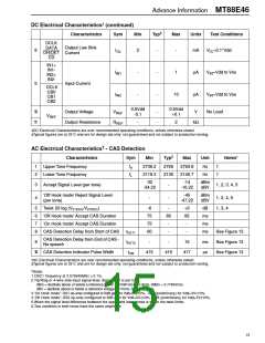
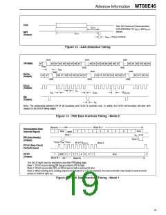
CAS
See ‘AC Electrical Characteristics -
t
DET2
CAS Detection’ for t
values.
and t
DET1
DET2
DET
(Output)
t
DET1
t
= 416µs nominal
DW
Figure 13 - CAS Detection Timing
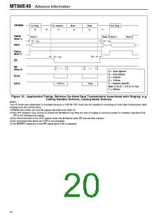
start
start
start
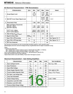
TIP/RING
b7
stop
b0 b1 b2 b3 b4 b5 b6 b7
b0 b1 b2 b3 b4 b5 b6 b7
b0 b1 b2 b3 b4 b5
stop
stop
t
IDD
start
start
start
b0 b1 b2 b3 b4 b5 b6 b7
DATA
(Output)
b6 b7
b0 b1 b2 b3 b4 b5 b6 b7
b0 b1 b2 b3
stop
stop
stop
DCLK
(Output)
t
CL
t
t
1/f
DCLK0
CH
CRD
DR
(Output)
t
RL
Note: The relationship between DATA bit boundary and DCLK is symbolic only. In reality, the DATA bit boundary will jitter with
respect to the DCLK falling edges.
Figure 14 - FSK Data Interface Timing - Mode 0
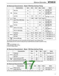
Word N+1
3
Word N
7
Demodulated Data
(Internal Signal)
1
5
stop
0
2
4
6
7
stop
start
Note 1
t
RL
DR (Data Ready)
(Output)
Note 2
>t
>t
DDS
DDH
1/f
4
Note 3
DCLK1
DCLK (Data Clock)
(Schmitt Input)
DATA
7
stop
0
1
2
3
5
6
7
stop
0
(Output)
Word N-1
Word N
The DCLK input must be low before and after DR falling edge.
Note 1: DCLK occurs during DR low and returns DR to high.
Note 2: DCLK occurs after DR, so DR is low for half a nominal bit time.
Note 3: When framing error (trailing stop bit a 0 instead of a 1) is not checked, the microcontroller only needs to send 8 DCLK
pulses to shift the byte out.
Figure 15 - FSK Data Interface Timing - Mode 1
19

 ZARLINK [ ZARLINK SEMICONDUCTOR INC ]