MT312 Tuner Control
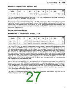
4.5.2 Frequency Error 1 and 2. Registers 111 - 115 (R)
Def
hex
NAME
ADR
B7
B6
B5
B4
B3
B2
B1
B0
FREQ ERR1 H
111
FREQ ERR1[23:16] Input frequency error coarse (high byte)
FREQ ERR1[15:8] Input frequency error coarse (middle byte)
FREQ ERR1[7:0] Input frequency error coarse (low byte)
R
R
R
00
00
00
FREQ ERR1 M 112
FREQ ERR1 L 113
24
FREQ ERR1[23:0] Ratio of Frequency Compensation Mixer offset to System Clock x 2 . 24 bit signed
number. For most purposes the LS byte can be ignored hence the alternative definition is more useful: FREQ
16
ERR1[23:8] Ratio of Frequency Compensation Mixer offset to System Clock x 2 . 16 bit signed number.
Def
hex
NAME
ADR
B7
B6
B5
B4
B3
B2
B1
B0
FREQ ERR2 H
FREQ ERR2 L
114
115
FREQ ERR2[15:8] Input frequency error fine (high byte)
FREQ ERR2[7:0] Input frequency error fine (low byte)
R
R
00
00
8
FREQ ERR2 [16:0] Ratio of Carrier Synchroniser offset to Symbol Rate x 2 . 16 bit signed number. This value
drops to near zero within a second or so of signal lock.
To obtain an accurate value for the frequency offset at any time, especially immediately after lock, the error
from each of these registers can be calculated and add together. In practice only the two most significant bytes
of FREQ ERR 1 are required, so that the net offset can be calculated as:
FREQ_ERR1(23:8)* PLL_CLK FREQ_ERR2(15:0)*Rs
Frequency offset = -------------------------------------------------------------------------------- + ------------------------------------------------------------
65536
256
Where PLL CLK is the sytem clock frequency (e.g. 60 MHz) and Rs is the symbol rate in MBd.
Any frequency error in FREQ ERR2 transfers to FREQ ERR1 very rapidly after lock, so that any delay between
reading the two values will cause an error in the calculation. It is therefore recommended that the five bytes
above are read as a block, especially if the two wire bus is subject to congestion or other delays.
28

 ZARLINK [ ZARLINK SEMICONDUCTOR INC ]