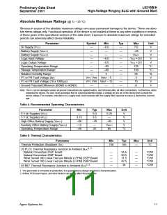
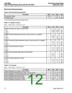
L9216B/H
Preliminary Data Sheet
September 2001
High-Voltage Ringing SLIC with Ground Start
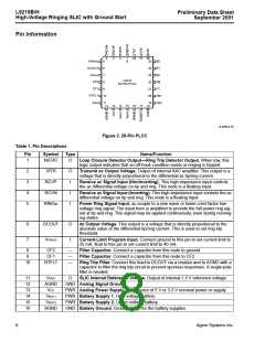
Pin Information (continued)
Table 1. Pin Descriptions (continued)
Pin
Symbol
Type
Name/Function
17
RGDET
O
Ring Ground Detect. When high, this open collector output indicates the pres-
ence of a ring ground or a tip ground. This supervision output may be used in
ground key, ground start or common-mode fault detection applications.
18
19
20
ICM
FB2
FB1
I
Common-Mode Current Sense. To program tip or ring ground sense threshold,
connect a resistor to VCC and connect a capacitor to AGND to filter 50/60 Hz. If
unused, the pin is connected to ground.
—
—
Polarity Reversal Slowdown Capacitor. Connect a capacitor from this node to
ground for controlling rate of battery reversal. If ramped battery reversal is not
desired, this pin is left open.
Polarity Reversal Slowdown Capacitor. Connect a capacitor from this node to
ground for controlling rate of battery reversal. If ramped battery reversal is not
desired, this pin is left open.
21
22
PT
I/O Protected Tip. The output drive of the tip amplifier and input to the loop-sensing
circuit. Connect to loop through overvoltage and overcurrent protection.
PR
I/O Protected Ring. The output drive of the ring amplifier and input to the loop-sens-
ing circuit. Connect to loop through overvoltage and overcurrent protection.
23
24
25
26
B2
B1
Id
Id
Id
I
State Control Input. These pins have an internal 110 kΩ pull-down.
B0
ITR
Transmit Gain. Input to AX amplifier. Connect a 4.75 kΩ resistor from this node to
VTX to set transmit gain. Gain shaping for termination impedance with a first-gen-
eration codec is also achieved with a network from this node to VTX.
27
28
VTX
TXI
O
I
ac Output Voltage. Output of internal AX amplifier. The voltage at this pin is
directly proportional to the differential tip/ring current.
ac/dc Separation. Input to internal AAC amplifier. Connect a 0.1 µF capacitor
from this pin to VTX.
Operating States
Table 2. Control States
B0
1
B1
1
B2
0
State
Forward active
1
0
0
Reverse active
1
1
1
On-hook transmission forward battery
On-hook transmission reverse battery
Ground start
1
0
1
0
0
1
0
1
1
Scan
0
0
0
Disconnect, device will power up in this state
Ring
0
1
0
Table 3. Supervision Coding
NSTAT
0 = off-hook or ring trip or TSD.
RGDET
0 = no ring or tip ground.
1 = on-hook and no ring trip and no TSD or DISCONNECT state. 1 = ring or tip ground.
Agere Systems Inc.
9

 ZARLINK [ ZARLINK SEMICONDUCTOR INC ]