L9216B/H
Preliminary Data Sheet
September 2001
High-Voltage Ringing SLIC with Ground Start
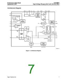
Pin Information
4
3
2
1
28 27 26
25
RINGIN
DCOUT
VPROG
CF2
5
6
7
8
9
B0
24
23
22
21
20
19
B1
B2
L9216
PR
PT
28-PIN PLCC
CF1
RTFLT
VREF
10
11
FB1
FB2
12 13 14 15 16 17 18
12-3558.d (F)
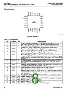
Figure 2. 28-Pin PLCC
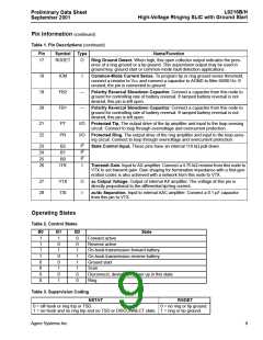
Table 1. Pin Descriptions
Pin
Symbol
Type
Name/Function
1
NSTAT
O
Loop Closure Detector Output—Ring Trip Detector Output. When low, this
logic output indicates that an off-hook condition exists or ringing is tripped.
2
3
4
5
VITR
RCVP
RCVN
RINGIN
O
I
Transmit ac Output Voltage. Output of internal AAC amplifier. This output is a
voltage that is directly proportional to the differential ac tip/ring current.
Receive ac Signal Input (Noninverting). This high-impedance input controls
the ac differential voltage on tip and ring. This node is a floating input.
I
Receive ac Signal Input (Inverting). This high-impedance input controls the ac
differential voltage on tip and ring. This node is a floating input.
I
Power Ring Signal Input. ac-couple to a sine wave or lower crest factor low-
voltage ring signal. The input here is amplified to provide the full power ring sig-
nal at tip and ring. This signal may be applied continuously, even during nonring-
ing states.
6
7
DCOUT
VPROG
O
I
dc Output Voltage. This output is a voltage that is directly proportional to the
absolute value of the differential tip/ring current. This is used to set ring trip
threshold.
Current-Limit Program Input. Connect ground to this pin to set current limit to
25 mA, float to this pin to set current limit to 40 mA.
8
9
CF2
CF1
—
—
—
Filter Capacitor. Connect a capacitor from this node to ground.
Filter Capacitor. Connect a capacitor from this node to CF2.
10
RTFLT
Ring Trip Filter. Connect this lead to DCOUT via a resistor and to AGND with a
capacitor to filter the ring trip circuit to prevent spurious responses. A single-pole
filter is needed.
11
12
13
14
15
16
VREF
AGND
VCC
O
SLIC Internal Reference Voltage. Output of internal 1.5 V reference voltage.
GND Analog Signal Ground.
PWR Analog Power Supply. User choice of 5 V or 3.3 V nominal power or supply.
PWR Battery Supply 1. High-voltage battery.
VBAT1
VBAT2
BGND
PWR Battery Supply 2. Lower-voltage battery.
GND Battery Ground. Ground return for the battery supplies.
8
Agere Systems Inc.

 ZARLINK [ ZARLINK SEMICONDUCTOR INC ]