L9216B/H
Preliminary Data Sheet
September 2001
High-Voltage Ringing SLIC with Ground Start
Table of Contents (continued)
Page Tables
Figures
Page
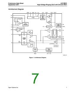
Figure 1. Architecture Diagram ...................................7
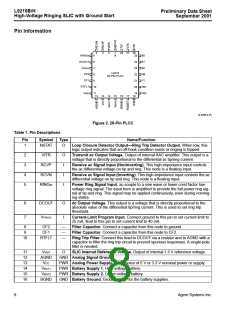
Figure 2. 28-Pin PLCC ...............................................8
Figure 3. Basic Test Circuit ......................................19
Figure 4. Metallic PSRR ...........................................20
Figure 5. Longitudinal PSRR ....................................20
Figure 6. Longitudinal Balance .................................20
Figure 7. ac Gains ....................................................20
Figure 8. Ringing Waveform Crest Factor = 1.6 .......24
Figure 9. Ringing Waveform Crest Factor = 1.2 .......24
Figure 10. Ring Mode Typical Operation ..................25
Figure 11. RINGIN Operation ....................................26
Figure 12. L9215/16 Ringing Input Circuit Selection
Table for Square Wave and PWM
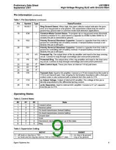
Table 1. Pin Descriptions .......................................... 8
Table 2. Operating States .......................................... 9
Table 3. Supervision Coding ..................................... 9
Table 4. Recommended Operating
Characteristics .......................................... 11
Table 5. Thermal Characteristics.............................. 11
Table 6. Environmental Characteristics.................... 12
Table 7. 5 V Supply Currents ................................... 12
Table 8. 5 V Powering .............................................. 12
Table 9. 3.3 V Supply Currents ................................ 13
Table 10. 3.3 V Powering ......................................... 13
Table 11. 2-Wire Port .............................................. 14
Table 12. Analog Pin Characteristics ..................... 15
Table 13. ac Feed Characteristics .......................... 16
Table 14. Logic Inputs and Outputs (VCC = 5 V) ..... 17
Table 15. Logic Inputs and Outputs (VCC = 3.3 V) .. 17
Table 16. Ground Start ............................................ 17
Table 17. Ringing Specifications ............................. 18
Table 18. Ring Trip .................................................. 18
Table 19. Typical Active Mode On- to Off-Hook
Tip/Ring Current-Limit Transient
Inputs .......................................................27
Figure 13. Modulation Waveforms ............................28
Figure 14. 5 V PWM Signal Amplitude .....................28
Figure 15. Ringing Output on RING, with
VCC = 5 V .................................................28
Figure 16. 3.3 V PWM Signal Amplitude ..................29
Figure 17. Ringing Output on RING, with
VCC = 3.1 V ..............................................29
Figure 18. Square Wave Input Signal and
Response ................................................ 22
Table 20. FB1 and FB2 Values vs. Typical Ramp
Time ......................................................... 23
Table 21. Onset of Power Ringing Clipping
VCC = 5 V, Cinput = 0.47 µF ................... 26
Table 22. Onset of Power Ringing Clipping
VCC = 3.1 V, Cinput = 0.47 µF ................ 26
Table 23. Signal and Component Selection Chart ... 27
Table 24. Parts List L9216; Agere T7504 First-
Generation Codec Resistive Termination;
Trapezoidal Power Ring Signal Output ...29
Figure 19. Crest Factor vs. Battery Voltage .............30
Figure 20. Crest Factor vs. R (kΩ) ...........................30
Figure 21. ac Equivalent Circuit ................................34
Figure 22. Agere T7504 First-Generation Codec
Resistive Termination ..............................34
Figure 23. Interface Circuit Using First-Generation
Codec (Blocking Capacitors Not
Shown) ....................................................37
Figure 24. ac Interface Using First-Generation Codec
(Including Blocking Capacitors) for
Nonmeter Pulse Application ................... 35
Table 25. Parts List L9216; Agere T7504 First-
Generation Codec Complex Termination;
Complex Termination Impedance ...........39
Figure 25. Agere T7504 First-Generation Codec
Complex Termination ..............................39
Meter Pulse Application ........................... 40
Table 26. Parts List L9216; Agere T8536
Figure 26. Third-Generation Codec ac Interface
Network; Complex Termination ...............41
Third-Generation Codec ac and
dc Parameters; Fully Programmable ...... 42
Agere Systems Inc.
3

 ZARLINK [ ZARLINK SEMICONDUCTOR INC ]