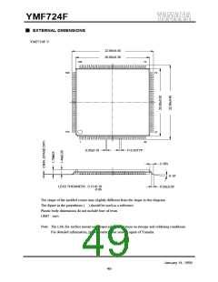
YMF724F
4-3. PCI Interface (Fig.3, 4)
Item
Symbol
Condition
Min.
Typ.
Max.
Unit
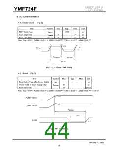
PCICLK Cycle Time
PCICLK High Time
PCICLK Low Time
PCICLK Slew Rate
tPCYC
tPHIGH
tPLOW
-
30
11
11
1
-
-
-
-
-
-
-
-
-
-
-
ns
ns
-
ns
4
V/ns
ns
tPVAL
(Bused signal)
2
11
12
-
PCICLK to Signal Valid Delay
tPVAL(PTP) (Point to Point)
2
ns
Float to Active Delay
Active to Float Delay
tPON
2
ns
tPOFF
-
28
-
ns
tPSU
tPSU(PTP)
tPH
(Bused signal)
7
ns
Input Setup Time to PCICLK
Input Hold Time for PCICLK
*10 (Point to Point)
*11 (Point to Point)
10
12
0
ns
-
-
-
-
ns
ns
Note : Top = 0-70°C, PVDD=5.0±0.25 V, VDD5=5.0±0.25 V, VDD3=3.3±0.3 V, LVDD=3.3±0.3 V, CL=50 pF
*10: This characteristic is applicable to REQ# and PCREQ# signal.
*11: This characteristic is applicable to GNT# and PCGNT# signal.
2.2 V
1.5 V
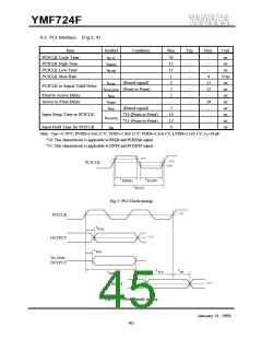
PCICLK
0.8 V
t
t
PLOW
PHIGH
t
PCYC
Fig.3: PCI Clock timing
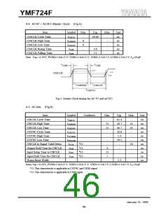
1.5 V
PCICLK
tPVAL
1.5 V
OUTPUT
tPON
Tri-State
OUTPUT
tPSU
tPH
tPOFF
1.5 V
INPUT
Fig.4: PCI Bus Signals timing
January 14, 1999
-45-

 YAMAHA [ YAMAHA CORPORATION ]