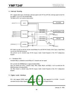
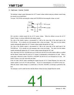
YMF724F
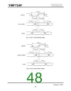
4. AC Characteristics
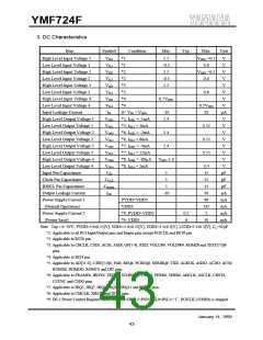
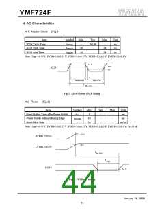
4-1. Master Clock (Fig.1)
Item
Symbol
Min.
Typ.
Max.
Unit
XI24 Cycle Time
XI24 High Time
XI24 Low Time
tXICYC
tXIHIGH
tXILOW
-
40.69
-
ns
ns
ns
16
16
-
-
24
24
Note : Top = 0-70°C, PVDD=5.0±0.25 V, VDD5=5.0±0.25 V, VDD3=3.3±0.3 V, LVDD=3.3±0.3 V
3.5 V
2.5 V
XI24
1.0 V
t
t
XIHIGH
XILOW
t
XICYC
Fig.1: XI24 Master Clock timing
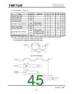
4-2. Reset (Fig.2)
Item
Symbol
Min.
Typ.
Max.
Unit
Reset Active Time after Power Stable
Power Stable to Reset Rising Edge
Reset Slew Rate
tRST
tRSTOFF
-
1
-
-
-
-
-
-
ms
ms
10
50
mV/ns
Note : Top = 0-70°C, PVDD=5.0±0.25 V, VDD5=5.0±0.25 V, VDD3=3.3±0.3 V, LVDD=3.3±0.3 V, CL=50 pF
4.75 V
PVDD, VDD5
3.0 V
LVDD, VDD3
tRSTOFF
tRST
RST#
0.6 V
Fig.2: PCI Reset timing
January 14, 1999
-44-

 YAMAHA [ YAMAHA CORPORATION ]