R
QPRO XQ4000E/EX QML High-Reliability FPGAs
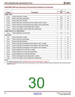
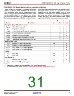
FXQ4028EX IOB Output Switching Characteristic Guidelines
Testing of switching parameters is modeled after testing
methods specified by MIL-M-38510/605. All devices are
100% functionally tested. Internal timing parameters are
derived from measuring internal test patterns. Listed below
are representative values. For more specific, more precise,
and worst-case guaranteed data, use the values reported
by the static timing analyzer (TRCE in the Xilinx Develop-
ment System) and back-annotated to the simulation netlist.
These path delays, provided as a guideline, have been
extracted from the static timing analyzer report. All timing
parameters assume worst-case operating conditions (sup-
ply voltage and junction temperature). For Propagation
Delays, slew-rate = fast unless otherwise noted. Values
apply to all XQ4000EX devices unless otherwise noted.
-4
Symbol
Description
Min
Max
Units
Propagation Delays (TTL Output Levels)
T
Clock (OK) to pad, fast
Output (O) to pad, fast
-
-
-
-
-
-
-
7.4
6.2
4.9
6.2
6.7
6.2
7.3
ns
ns
ns
ns
ns
OKPOF
T
OPF
T
3-state to pad High-Z, slew-rate independent
3-state to pad active and valid, fast
TSHZ
TSONF
OKFPF
CEFPF
T
T
T
Output MUX select (OK) to pad
Fast path output MUX input (EC) to pad
Slowest path output MUX input (EC) to pad
T
OFPF
Setup and Hold Times
T
Output (O) to clock (OK) setup time
Output (O) to clock (OK) hold time
Clock enable (EC) to clock (OK) setup
Clock enable (EC) to clock (OK) hold
0.6
0
-
-
-
-
ns
ns
ns
ns
OOK
T
OKO
T
T
0
ECOK
OKEC
0
Clocks
T
Clock High
Clock Low
3.5
3.5
-
-
ns
ns
CH
T
CL
Global Set/Reset
T
Minimum GSR pulse width
13.0
30.2
-
-
ns
ns
MRW
T
Delay from GSR input to any pad
RRI
Notes:
1. Output timing is measured at TTL threshold, with 35 pF external capacitive loads.
2. For CMOS output levels, see the "XQ4028EX Output Level and Slew Rate Adjustments" on page 27.
DS021 (v2.2) June 25, 2000
www.xilinx.com
31
Product Specification
1-800-255-7778

 XILINX [ XILINX, INC ]