R
Spartan-II FPGA Family: Functional Description
At the third rising edge of CLKA, the TBCCS parameter is
violated with two writes to memory location 0x0F. The DOA
and DOB busses reflect the contents of the DIA and DIB
busses, but the stored value at 0x7E is invalid.
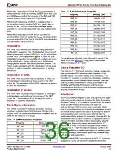
Table 14: RAM Initialization Properties
Property
INIT_05
INIT_06
INIT_07
INIT_08
INIT_09
INIT_0a
INIT_0b
INIT_0c
INIT_0d
INIT_0e
INIT_0f
Memory Cells
1535 to 1280
1791 to 1536
2047 to 1792
2303 to 2048
2559 to 2304
2815 to 2560
3071 to 2816
3327 to 3072
3583 to 3328
3839 to 3584
4095 to 3840
At the fourth rising edge of CLKA, a read operation is
performed at memory location 0x0F and invalid data is
present on the DOA bus. Port B also executes a read
operation to memory location 0x0F and also reads invalid
data.
At the fifth rising edge of CLKA a read operation is
performed that does not violate the TBCCS parameter to the
previous write of 0x7E by Port B. THe DOA bus reflects the
recently written value by Port B.
Initialization
The block RAM memory can initialize during the device
configuration sequence. The 16 initialization properties of
64 hex values each (a total of 4096 bits) set the initialization
of each RAM. These properties appear in Table 14. Any
initialization properties not explicitly set configure as zeros.
Partial initialization strings pad with zeros. Initialization
strings greater than 64 hex values generate an error. The
RAMs can be simulated with the initialization values using
generics in VHDL simulators and parameters in Verilog
simulators.
For design examples and more information on using the
Block RAM, see XAPP173, Using Block SelectRAM+
Memory in Spartan-II FPGAs.
Using Versatile I/O
The Spartan-II FPGA family includes a highly configurable,
high-performance I/O resource called Versatile I/O to
provide support for a wide variety of I/O standards. The
Versatile I/O resource is a robust set of features including
programmable control of output drive strength, slew rate,
and input delay and hold time. Taking advantage of the
flexibility and Versatile I/O features and the design
considerations described in this document can improve and
simplify system level design.
Initialization in VHDL
The block RAM structures may be initialized in VHDL for
both simulation and synthesis for inclusion in the EDIF
output file. The simulation of the VHDL code uses a generic
to pass the initialization.
Initialization in Verilog
The block RAM structures may be initialized in Verilog for
both simulation and synthesis for inclusion in the EDIF
output file. The simulation of the Verilog code uses a
defparam to pass the initialization.
Introduction
As FPGAs continue to grow in size and capacity, the larger
and more complex systems designed for them demand an
increased variety of I/O standards. Furthermore, as system
clock speeds continue to increase, the need for
Block Memory Generation
high-performance I/O becomes more important. While
chip-to-chip delays have an increasingly substantial impact
on overall system speed, the task of achieving the desired
system performance becomes more difficult with the
proliferation of low-voltage I/O standards. Versatile I/O, the
revolutionary input/output resources of Spartan-II devices,
has resolved this potential problem by providing a highly
configurable, high-performance alternative to the I/O
resources of more conventional programmable devices.
The Spartan-II FPGA Versatile I/O features combine the
flexibility and time-to-market advantages of programmable
logic with the high performance previously available only
with ASICs and custom ICs.
The CORE Generator™ software generates memory
structures using the block RAM features. This program
outputs VHDL or Verilog simulation code templates and an
EDIF file for inclusion in a design.
Table 14: RAM Initialization Properties
Property
INIT_00
INIT_01
INIT_02
INIT_03
INIT_04
Memory Cells
255 to 0
511 to 256
767 to 512
1023 to 768
1279 to 1024
Each Versatile I/O block can support up to 16 I/O standards.
Supporting such a variety of I/O standards allows the
DS001-2 (v2.8) June 13, 2008
Product Specification
www.xilinx.com
Module 2 of 4
36

 XILINX [ XILINX, INC ]