6
Spartan-II FPGA Family:
Introduction and Ordering
Information
R
0
DS001-1 (v2.8) June 13, 2008
Product Specification
•
System level features
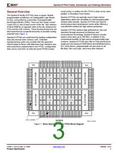
Introduction
The Spartan®-II Field-Programmable Gate Array family
gives users high performance, abundant logic resources,
and a rich feature set, all at an exceptionally low price. The
six-member family offers densities ranging from 15,000 to
200,000 system gates, as shown in Table 1. System
performance is supported up to 200 MHz. Features include
block RAM (to 56K bits), distributed RAM (to 75,264 bits),
16 selectable I/O standards, and four DLLs. Fast,
-
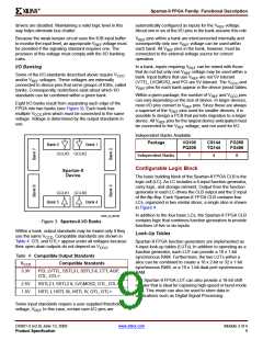
SelectRAM™ hierarchical memory:
·
·
·
16 bits/LUT distributed RAM
Configurable 4K bit block RAM
Fast interfaces to external RAM
-
-
-
-
-
-
-
-
-
Fully PCI compliant
Low-power segmented routing architecture
Full readback ability for verification/observability
Dedicated carry logic for high-speed arithmetic
Efficient multiplier support
Cascade chain for wide-input functions
Abundant registers/latches with enable, set, reset
Four dedicated DLLs for advanced clock control
Four primary low-skew global clock distribution
nets
predictable interconnect means that successive design
iterations continue to meet timing requirements.
The Spartan-II family is a superior alternative to
mask-programmed ASICs. The FPGA avoids the initial
cost, lengthy development cycles, and inherent risk of
conventional ASICs. Also, FPGA programmability permits
design upgrades in the field with no hardware replacement
necessary (impossible with ASICs).
-
IEEE 1149.1 compatible boundary scan logic
•
Versatile I/O and packaging
-
-
-
-
-
-
Pb-free package options
Low-cost packages available in all densities
Family footprint compatibility in common packages
16 high-performance interface standards
Hot swap Compact PCI friendly
Features
•
Second generation ASIC replacement technology
-
Densities as high as 5,292 logic cells with up to
200,000 system gates
Zero hold time simplifies system timing
-
Streamlined features based on Virtex® FPGA
architecture
•
•
Core logic powered at 2.5V and I/Os powered at 1.5V,
2.5V, or 3.3V
Fully supported by powerful Xilinx® ISE® development
system
-
-
-
Unlimited reprogrammability
Very low cost
Cost-effective 0.18 micron process
-
Fully automatic mapping, placement, and routing
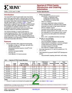
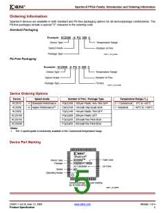
Table 1: Spartan-II FPGA Family Members
CLB
Array
(R x C)
Maximum
Available
User I/O(1)
Total
Total
Logic
Cells
System Gates
(Logic and RAM)
Total
CLBs
Distributed RAM Block RAM
Device
XC2S15
XC2S30
XC2S50
XC2S100
XC2S150
XC2S200
Bits
Bits
16K
24K
32K
40K
48K
56K
432
15,000
30,000
8 x 12
12 x 18
16 x 24
20 x 30
24 x 36
28 x 42
96
86
6,144
972
216
92
13,824
24,576
38,400
55,296
75,264
1,728
2,700
3,888
5,292
50,000
384
176
176
260
284
100,000
150,000
200,000
600
864
1,176
Notes:
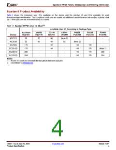
1. All user I/O counts do not include the four global clock/user input pins. See details in Table 2, page 4.
© 2000-2008 Xilinx, Inc. All rights reserved. XILINX, the Xilinx logo, the Brand Window, and other designated brands included herein are trademarks of Xilinx, Inc. All other
trademarks are the property of their respective owners.
DS001-1 (v2.8) June 13, 2008
Product Specification
www.xilinx.com
Module 1 of 4
2

 XILINX [ XILINX, INC ]