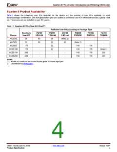
R
Spartan-II FPGA Family: Functional Description
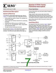
The three IOB registers function either as edge-triggered
D-type flip-flops or as level-sensitive latches. Each IOB has
a clock signal (CLK) shared by the three registers and
independent Clock Enable (CE) signals for each register. In
addition to the CLK and CE control signals, the three
registers share a Set/Reset (SR). For each register, this
signal can be independently configured as a synchronous
Set, a synchronous Reset, an asynchronous Preset, or an
asynchronous Clear.
All pads are protected against damage from electrostatic
discharge (ESD) and from over-voltage transients. Two
forms of over-voltage protection are provided, one that
permits 5V compliance, and one that does not. For 5V
compliance, a zener-like structure connected to ground
turns on when the output rises to approximately 6.5V. When
5V compliance is not required, a conventional clamp diode
may be connected to the output supply voltage, VCCO. The
type of over-voltage protection can be selected
independently for each pad.
A feature not shown in the block diagram, but controlled by
the software, is polarity control. The input and output buffers
and all of the IOB control signals have independent polarity
controls.
All Spartan-II FPGA IOBs support IEEE 1149.1-compatible
boundary scan testing.
Input Path
Optional pull-up and pull-down resistors and an optional
weak-keeper circuit are attached to each pad. Prior to
configuration all outputs not involved in configuration are
forced into their high-impedance state. The pull-down
resistors and the weak-keeper circuits are inactive, but
inputs may optionally be pulled up.
A buffer In the Spartan-II FPGA IOB input path routes the
input signal either directly to internal logic or through an
optional input flip-flop.
An optional delay element at the D-input of this flip-flop
eliminates pad-to-pad hold time. The delay is matched to
the internal clock-distribution delay of the FPGA, and when
used, assures that the pad-to-pad hold time is zero.
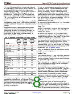
Table 3: Standards Supported by I/O (Typical Values)
Input
Reference Source Termination
Voltage Voltage Voltage
Output
Board
Each input buffer can be configured to conform to any of the
low-voltage signaling standards supported. In some of
these standards the input buffer utilizes a user-supplied
threshold voltage, VREF. The need to supply VREF imposes
constraints on which standards can used in close proximity
to each other. See "I/O Banking," page 9.
I/O Standard
LVTTL (2-24 mA)
LVCMOS2
(VREF
)
(VCCO
)
(VTT
N/A
N/A
N/A
)
N/A
3.3
N/A
2.5
There are optional pull-up and pull-down resistors at each
input for use after configuration.
PCI (3V/5V,
N/A
3.3
33 MHz/66 MHz)
Output Path
GTL
0.8
1.0
N/A
N/A
1.5
1.5
1.5
3.3
1.2
1.5
The output path includes a 3-state output buffer that drives
the output signal onto the pad. The output signal can be
routed to the buffer directly from the internal logic or through
an optional IOB output flip-flop.
GTL+
HSTL Class I
HSTL Class III
HSTL Class IV
0.75
0.9
0.75
1.5
1.5
1.5
The 3-state control of the output can also be routed directly
from the internal logic or through a flip-flip that provides
synchronous enable and disable.
0.9
SSTL3 Class I
and II
1.5
Each output driver can be individually programmed for a
wide range of low-voltage signaling standards. Each output
buffer can source up to 24 mA and sink up to 48 mA. Drive
strength and slew rate controls minimize bus transients.
SSTL2 Class I
and II
1.25
2.5
1.25
CTT
1.5
3.3
3.3
1.5
In most signaling standards, the output high voltage
depends on an externally supplied VCCO voltage. The need
to supply VCCO imposes constraints on which standards
can be used in close proximity to each other. See "I/O
Banking".
AGP-2X
1.32
N/A
The activation of pull-up resistors prior to configuration is
controlled on a global basis by the configuration mode pins.
If the pull-up resistors are not activated, all the pins will float.
Consequently, external pull-up or pull-down resistors must
be provided on pins required to be at a well-defined logic
level prior to configuration.
An optional weak-keeper circuit is connected to each
output. When selected, the circuit monitors the voltage on
the pad and weakly drives the pin High or Low to match the
input signal. If the pin is connected to a multiple-source
signal, the weak keeper holds the signal in its last state if all
DS001-2 (v2.8) June 13, 2008
Product Specification
www.xilinx.com
Module 2 of 4
8

 XILINX [ XILINX, INC ]