50
R
Spartan-II FPGA Family:
Functional Description
DS001-2 (v2.8) June 13, 2008
Product Specification
memory elements for easy and quick routing of signals on
and off the chip.
Architectural Description
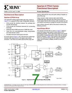
Spartan-II FPGA Array
Values stored in static memory cells control all the
The Spartan®-II field-programmable gate array, shown in
Figure 2, is composed of five major configurable elements:
configurable logic elements and interconnect resources.
These values load into the memory cells on power-up, and
can reload if necessary to change the function of the device.
•
IOBs provide the interface between the package pins
and the internal logic
Each of these elements will be discussed in detail in the
following sections.
•
CLBs provide the functional elements for constructing
most logic
Input/Output Block
•
•
Dedicated block RAM memories of 4096 bits each
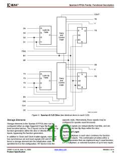
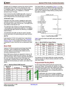
The Spartan-II FPGA IOB, as seen in Figure 2, features
inputs and outputs that support a wide variety of I/O
signaling standards. These high-speed inputs and outputs
are capable of supporting various state of the art memory
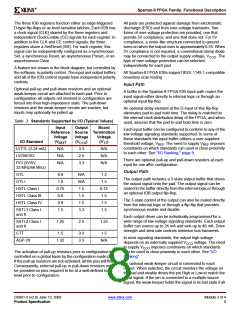
and bus interfaces. Table 3 lists several of the standards
which are supported along with the required reference,
output and termination voltages needed to meet the
standard.
Clock DLLs for clock-distribution delay compensation
and clock domain control
•
Versatile multi-level interconnect structure
As can be seen in Figure 2, the CLBs form the central logic
structure with easy access to all support and routing
structures. The IOBs are located around all the logic and
T
SR
V
CCO
D
Q
Package
Pin
TFF
CLK
TCE
SR
CK
EC
VCC
OE
I/O
Programmable
Bias &
ESD Network
Package Pin
SR
O
D
Q
Programmable
Output Buffer
OFF
CK
EC
Internal
Reference
OCE
Programmable
Delay
IQ
I
I/O, V
REF
SR
Programmable
Input Buffer
Package Pin
D
Q
IFF
CK
EC
To Next I/O
To Other
External V
Inputs
ICE
REF
of Bank
DS001_02_090600
Figure 2: Spartan-II FPGA Input/Output Block (IOB)
© 2000-2008 Xilinx, Inc. All rights reserved. XILINX, the Xilinx logo, the Brand Window, and other designated brands included herein are trademarks of Xilinx, Inc. All other
trademarks are the property of their respective owners.
DS001-2 (v2.8) June 13, 2008
Product Specification
www.xilinx.com
Module 2 of 4
7

 XILINX [ XILINX, INC ]