R
Spartan-II FPGA Family: Functional Description
drivers are disabled. Maintaining a valid logic level in this
way helps eliminate bus chatter.
automatically configured as inputs for the VREF voltage.
About one in six of the I/O pins in the bank assume this role.
Because the weak-keeper circuit uses the IOB input buffer
to monitor the input level, an appropriate VREF voltage must
be provided if the signaling standard requires one. The
provision of this voltage must comply with the I/O banking
rules.
VREF pins within a bank are interconnected internally and
consequently only one VREF voltage can be used within
each bank. All VREF pins in the bank, however, must be
connected to the external voltage source for correct
operation.
In a bank, inputs requiring VREF can be mixed with those
that do not but only one VREF voltage may be used within a
bank. Input buffers that use VREF are not 5V tolerant.
LVTTL, LVCMOS2, and PCI are 5V tolerant. The VCCO and
VREF pins for each bank appear in the device pinout tables.
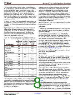
I/O Banking
Some of the I/O standards described above require VCCO
and/or VREF voltages. These voltages are externally
connected to device pins that serve groups of IOBs, called
banks. Consequently, restrictions exist about which I/O
standards can be combined within a given bank.
Within a given package, the number of VREF and VCCO pins
can vary depending on the size of device. In larger devices,
more I/O pins convert to VREF pins. Since these are always
a superset of the VREF pins used for smaller devices, it is
possible to design a PCB that permits migration to a larger
device. All VREF pins for the largest device anticipated must
be connected to the VREF voltage, and not used for I/O.
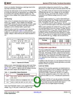
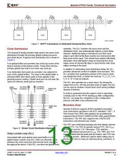
Eight I/O banks result from separating each edge of the
FPGA into two banks (see Figure 3). Each bank has
multiple VCCO pins which must be connected to the same
voltage. Voltage is determined by the output standards in
use.
Independent Banks Available
Package
VQ100
PQ208
CS144
TQ144
FG256
FG456
Bank 0
Bank 1
GCLK3 GCLK2
Independent Banks
1
4
8
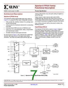
Configurable Logic Block
Spartan-II
Device
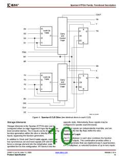
The basic building block of the Spartan-II FPGA CLB is the
logic cell (LC). An LC includes a 4-input function generator,
carry logic, and storage element. Output from the function
generator in each LC drives the CLB output and the D input
of the flip-flop. Each Spartan-II FPGA CLB contains four
LCs, organized in two similar slices; a single slice is shown
in Figure 4.
GCLK1 GCLK0
Bank 5
Bank 4
In addition to the four basic LCs, the Spartan-II FPGA CLB
contains logic that combines function generators to provide
functions of five or six inputs.
DS001_03_060100
Figure 3: Spartan-II I/O Banks
Within a bank, output standards may be mixed only if they
use the same VCCO. Compatible standards are shown in
Table 4. GTL and GTL+ appear under all voltages because
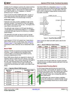
Look-Up Tables
Spartan-II FPGA function generators are implemented as
4-input look-up tables (LUTs). In addition to operating as a
function generator, each LUT can provide a 16 x 1-bit
synchronous RAM. Furthermore, the two LUTs within a
slice can be combined to create a 16 x 2-bit or 32 x 1-bit
synchronous RAM, or a 16 x 1-bit dual-port synchronous
RAM.
their open-drain outputs do not depend on VCCO
.
Table 4: Compatible Output Standards
VCCO
Compatible Standards
3.3V
PCI, LVTTL, SSTL3 I, SSTL3 II, CTT, AGP,
GTL, GTL+
The Spartan-II FPGA LUT can also provide a 16-bit shift
register that is ideal for capturing high-speed or burst-mode
data. This mode can also be used to store data in
applications such as Digital Signal Processing.
2.5V
1.5V
SSTL2 I, SSTL2 II, LVCMOS2, GTL, GTL+
HSTL I, HSTL III, HSTL IV, GTL, GTL+
Some input standards require a user-supplied threshold
voltage, VREF. In this case, certain user-I/O pins are
DS001-2 (v2.8) June 13, 2008
Product Specification
www.xilinx.com
Module 2 of 4
9

 XILINX [ XILINX, INC ]