Artix-7 FPGAs Data Sheet: DC and AC Switching Characteristics
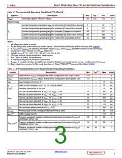
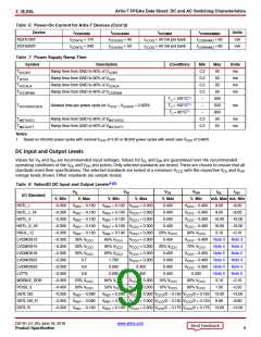
Table 3: DC Characteristics Over Recommended Operating Conditions (Cont’d)
Symbol Description
Min
–
Typ(1)
1.010
2
Max
Units
n
r
Temperature diode ideality factor
Temperature diode series resistance
–
–
–
–
Ω
Notes:
1. Typical values are specified at nominal voltage, 25°C.
2. This measurement represents the die capacitance at the pad, not including the package.
3. Maximum value specified for worst case process at 25°C.
4. Termination resistance to a V
/2 level.
CCO
(1)(2)
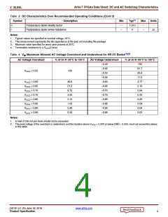
Table 4: V Maximum Allowed AC Voltage Overshoot and Undershoot for HR I/O Banks
IN
AC Voltage Overshoot
% of UI @–55°C to 125°C
AC Voltage Undershoot
% of UI @–55°C to 125°C
–0.40
–0.45
–0.50
–0.55
–0.60
–0.65
–0.70
–0.75
–0.80
–0.85
–0.90
–0.95
100
61.7
25.8
11.0
4.77
2.10
0.94
0.43
0.20
0.09
0.04
0.02
VCCO + 0.55
100
VCCO + 0.60
46.6
21.2
9.75
4.55
2.15
1.02
0.49
0.24
VCCO + 0.65
V
CCO + 0.70
CCO + 0.75
V
VCCO + 0.80
V
CCO + 0.85
CCO + 0.90
V
VCCO + 0.95
Notes:
1. A total of 200 mA per bank should not be exceeded.
2. The peak voltage of the overshoot or undershoot, and the duration above V
in this table.
+ 0.20V or below GND – 0.20V, must not exceed the values
CCO
DS181 (v1.25) June 18, 2018
www.xilinx.com
Product Specification
4

 XILINX [ XILINX, INC ]