Artix-7 FPGAs Data Sheet: DC and AC Switching Characteristics
(1)(2)
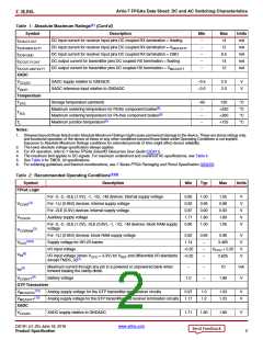
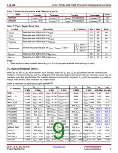
Table 2: Recommended Operating Conditions
Symbol Description
VREFP Externally supplied reference voltage
(Cont’d)
Min
Typ
Max
Units
1.20
1.25
1.30
V
Temperature
Junction temperature operating range for commercial (C) temperature devices
Junction temperature operating range for extended (E) temperature devices
Junction temperature operating range for industrial (I) temperature devices
Junction temperature operating range for expanded (Q) temperature devices
Junction temperature operating range for military (M) temperature devices
0
–
–
–
–
–
85
°C
°C
°C
°C
°C
0
100
100
125
125
Tj
–40
–40
–55
Notes:
1. All voltages are relative to ground.
2. For the design of the power distribution system consult 7 Series FPGAs PCB Design and Pin Planning Guide (UG483).
3. If V and V are operating at the same voltage, V and V should be connected to the same supply.
CCINT
CCBRAM
CCINT
CCBRAM
4. Configuration data is retained even if V
drops to 0V.
CCO
5. Includes V
of 1.2V, 1.35V, 1.5V, 1.8V, 2.5V, and 3.3V at 5ꢀ.
CCO
6. The lower absolute voltage specification always applies.
7. See Table 9 for TMDS_33 specifications.
8. A total of 200 mA per bank should not be exceeded.
9.
V
is required only when using bitstream encryption. If battery is not used, connect V
to either ground or V
.
CCBATT
CCBATT
CCAUX
10. Each voltage listed requires the filter circuit described in 7 Series FPGAs GTP Transceiver User Guide (UG482).
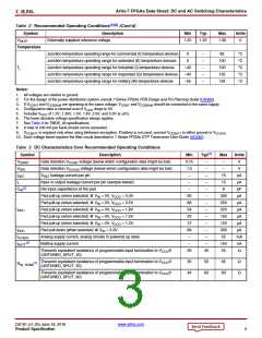
Table 3: DC Characteristics Over Recommended Operating Conditions
Symbol
VDRINT
Description
Data retention VCCINT voltage (below which configuration data might be lost)
Data retention VCCAUX voltage (below which configuration data might be lost)
VREF leakage current per pin
Min
0.75
1.5
–
Typ(1)
Max
–
Units
V
–
–
VDRI
IREF
IL
–
V
–
15
µA
µA
pF
µA
µA
µA
µA
µA
µA
mA
nA
Ω
Input or output leakage current per pin (sample-tested)
Die input capacitance at the pad
–
–
15
(2)
CIN
–
–
8
Pad pull-up (when selected) @ VIN = 0V, VCCO = 3.3V
Pad pull-up (when selected) @ VIN = 0V, VCCO = 2.5V
Pad pull-up (when selected) @ VIN = 0V, VCCO = 1.8V
Pad pull-up (when selected) @ VIN = 0V, VCCO = 1.5V
Pad pull-up (when selected) @ VIN = 0V, VCCO = 1.2V
Pad pull-down (when selected) @ VIN = 3.3V
90
68
34
23
12
68
–
–
330
250
220
150
120
330
25
–
IRPU
–
–
–
IRPD
–
ICCADC
Analog supply current, analog circuits in powered up state
Battery supply current
–
(3)
IBATT
–
–
150
55
Thevenin equivalent resistance of programmable input termination to VCCO/2
(UNTUNED_SPLIT_40)
28
40
Thevenin equivalent resistance of programmable input termination to VCCO/2
(UNTUNED_SPLIT_50)
35
44
50
60
65
83
Ω
Ω
(4)
RIN_TERM
Thevenin equivalent resistance of programmable input termination to VCCO/2
(UNTUNED_SPLIT_60)
DS181 (v1.25) June 18, 2018
www.xilinx.com
Product Specification
3

 XILINX [ XILINX, INC ]