Artix-7 FPGAs Data Sheet: DC and AC Switching Characteristics
(1)
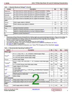
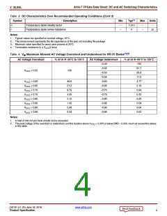
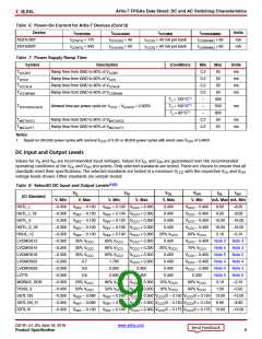
Table 1: Absolute Maximum Ratings (Cont’d)
Symbol
IDCIN-FLOAT
IDCIN-MGTAVTT
IDCIN-GND
Description
Min
–
Max
14
Units
mA
DC input current for receiver input pins DC coupled RX termination = floating
DC input current for receiver input pins DC coupled RX termination = VMGTAVTT
DC input current for receiver input pins DC coupled RX termination = GND
DC output current for transmitter pins DC coupled RX termination = floating
DC output current for transmitter pins DC coupled RX termination = VMGTAVTT
–
12
mA
–
6.5
14
mA
–
IDCOUT-FLOAT
IDCOUT-MGTAVTT
XADC
mA
–
12
mA
XADC supply relative to GNDADC
–0.5
–0.5
2.0
2.0
V
V
VCCADC
XADC reference input relative to GNDADC
VREFP
Temperature
TSTG
Storage temperature (ambient)
–65
–
150
°C
°C
°C
°C
Maximum soldering temperature for Pb/Sn component bodies(6)
Maximum soldering temperature for Pb-free component bodies(6)
Maximum junction temperature(6)
+220
+260
+125
TSOL
–
–
Tj
Notes:
1. Stresses beyond those listed under Absolute Maximum Ratings might cause permanent damage to the device. These are stress ratings only,
and functional operation of the device at these or any other conditions beyond those listed under Operating Conditions is not implied.
Exposure to Absolute Maximum Ratings conditions for extended periods of time might affect device reliability.
2. The lower absolute voltage specification always applies.
3. For I/O operation, refer to 7 Series FPGAs SelectIO Resources User Guide (UG471).
4. The maximum limit applies to DC signals. For maximum undershoot and overshoot AC specifications, see Table 4.
5. See Table 9 for TMDS_33 specifications.
6. For soldering guidelines and thermal considerations, see 7 Series FPGA Packaging and Pinout Specification (UG475).
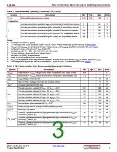
(1)(2)
Table 2: Recommended Operating Conditions
Symbol
Description
Min
Typ
Max
Units
FPGA Logic
For -3, -2, -2LE (1.0V), -1, -1Q, -1M devices: internal supply voltage
For -1LI (0.95V) devices: internal supply voltage
For -2LE (0.9V) devices: internal supply voltage
Auxiliary supply voltage
0.95
0.92
0.87
1.71
0.95
1.00
0.95
0.90
1.80
1.00
1.05
0.98
0.93
1.89
1.05
V
V
V
V
V
(3)
VCCINT
VCCAUX
For -3, -2, -2LE (1.0V), -2LE (0.9V), -1, -1Q, -1M devices: block RAM supply
voltage
(3)
VCCBRAM
For -1LI (0.95V) devices: block RAM supply voltage
Supply voltage for HR I/O banks
I/O input voltage
0.92
1.14
0.95
0.98
3.465
V
V
V
V
(4)(5)
VCCO
–
–
–
–0.20
–0.20
VCCO + 0.20
2.625
(6)
VIN
I/O input voltage (when VCCO = 3.3V) for VREF and differential I/O standards
except TMDS_33(7)
Maximum current through any pin in a powered or unpowered bank when
forward biasing the clamp diode.
–
–
–
10
mA
V
(8)
IIN
(9)
VCCBATT
Battery voltage
1.0
1.89
GTP Transceiver
(10)
VMGTAVCC
Analog supply voltage for the GTP transmitter and receiver circuits
0.97
1.17
1.0
1.2
1.03
1.23
V
V
(10)
VMGTAVTT
Analog supply voltage for the GTP transmitter and receiver termination circuits
XADC
VCCADC
XADC supply relative to GNDADC
1.71
1.80
1.89
V
DS181 (v1.25) June 18, 2018
www.xilinx.com
Product Specification
2

 XILINX [ XILINX, INC ]