Artix-7 FPGAs Data Sheet: DC and AC Switching Characteristics
IOB Pad Input/Output/3-State
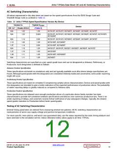
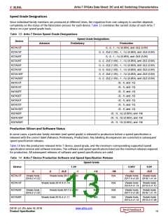
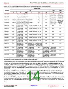
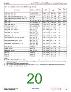
Table 17 summarizes the values of standard-specific data input delay adjustments, output delays terminating at pads (based
on standard) and 3-state delays.
•
•
•
T
is described as the delay from IOB pad through the input buffer to the I-pin of an IOB pad. The delay varies
IOPI
depending on the capability of the SelectIO input buffer.
T
is described as the delay from the O pin to the IOB pad through the output buffer of an IOB pad. The delay varies
IOOP
depending on the capability of the SelectIO output buffer.
T
is described as the delay from the T pin to the IOB pad through the output buffer of an IOB pad, when 3-state is
IOTP
disabled. The delay varies depending on the SelectIO capability of the output buffer. In HR I/O banks, the IN_TERM
termination turn-on time is always faster than T when the INTERMDISABLE pin is used.
IOTP
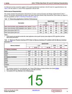
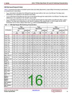
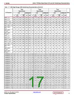
Table 17: IOB High Range (HR) Switching Characteristics
T
T
T
IOTP
IOPI
IOOP
Speed Grade
1.0V
Speed Grade
1.0V
Speed Grade
1.0V
I/O Standard
Units
0.95V 0.9V
0.95V 0.9V
0.95V 0.9V
-1LI -2LE
-2/
-1Q/
-1M
-2/
-1Q/
-1M
-2/
-1Q/
-1M
-3
-1
-1LI -2LE -3
-1
-1LI -2LE -3
-1
-2LE
-2LE
-2LE
LVTTL_S4
LVTTL_S8
LVTTL_S12
LVTTL_S16
LVTTL_S24
LVTTL_F4
LVTTL_F8
LVTTL_F12
LVTTL_F16
LVTTL_F24
LVDS_25
1.26 1.34 1.41 1.53 1.41 1.58 3.80 3.93 4.18 4.18 4.18 4.41 3.82 3.96 4.20 4.20 4.20 4.05 ns
1.26 1.34 1.41 1.53 1.41 1.58 3.54 3.66 3.92 3.92 3.92 4.15 3.56 3.69 3.93 3.93 3.93 3.78 ns
1.26 1.34 1.41 1.53 1.41 1.58 3.52 3.65 3.90 3.90 3.90 4.13 3.54 3.68 3.91 3.91 3.91 3.77 ns
1.26 1.34 1.41 1.53 1.41 1.58 3.07 3.19 3.45 3.45 3.45 3.68 3.09 3.22 3.46 3.46 3.46 3.31 ns
1.26 1.34 1.41 1.53 1.41 1.58 3.29 3.41 3.67 3.67 3.67 3.90 3.31 3.44 3.68 3.68 3.68 3.53 ns
1.26 1.34 1.41 1.53 1.41 1.58 3.26 3.38 3.64 3.64 3.64 3.86 3.28 3.41 3.65 3.65 3.65 3.50 ns
1.26 1.34 1.41 1.53 1.41 1.58 2.74 2.87 3.12 3.12 3.12 3.35 2.76 2.90 3.13 3.13 3.13 2.99 ns
1.26 1.34 1.41 1.53 1.41 1.58 2.73 2.85 3.10 3.10 3.10 3.33 2.74 2.88 3.12 3.12 3.12 2.97 ns
1.26 1.34 1.41 1.53 1.41 1.58 2.56 2.68 2.93 2.93 2.93 3.16 2.57 2.71 2.95 2.95 2.95 2.80 ns
1.26 1.34 1.41 1.53 1.41 1.58 2.52 2.65 2.90 3.23 2.90 3.22 2.54 2.68 2.91 3.24 2.91 2.86 ns
0.73 0.81 0.88 0.89 0.88 0.90 1.29 1.41 1.67 1.67 1.67 1.86 1.31 1.44 1.68 1.68 1.68 1.50 ns
MINI_LVDS_25 0.73 0.81 0.88 0.89 0.88 0.90 1.27 1.40 1.65 1.65 1.65 1.88 1.29 1.43 1.66 1.66 1.66 1.52 ns
BLVDS_25
0.73 0.81 0.88 0.88 0.88 0.90 1.84 1.96 2.21 2.76 2.21 2.44 1.85 1.99 2.23 2.77 2.23 2.08 ns
0.73 0.81 0.88 0.89 0.88 0.90 1.27 1.40 1.65 1.65 1.65 1.88 1.29 1.43 1.66 1.66 1.66 1.52 ns
RSDS_25 (point
to point)
PPDS_25
TMDS_33
PCI33_3
0.73 0.81 0.88 0.89 0.88 0.90 1.29 1.41 1.67 1.67 1.67 1.88 1.31 1.44 1.68 1.68 1.68 1.52 ns
0.73 0.81 0.88 0.92 0.88 0.90 1.41 1.54 1.79 1.79 1.79 1.99 1.43 1.57 1.80 1.80 1.80 1.63 ns
1.24 1.32 1.39 1.52 1.39 1.57 3.10 3.22 3.48 3.48 3.48 3.71 3.12 3.25 3.49 3.49 3.49 3.34 ns
0.67 0.75 0.82 0.88 0.82 0.87 1.81 1.93 2.18 2.18 2.18 2.41 1.82 1.96 2.20 2.20 2.20 2.05 ns
0.67 0.75 0.82 0.88 0.82 0.87 1.29 1.41 1.67 1.67 1.67 1.90 1.31 1.44 1.68 1.68 1.68 1.53 ns
HSUL_12_S
HSUL_12_F
DIFF_HSUL_
12_S
0.68 0.76 0.83 0.86 0.83 0.88 1.81 1.93 2.18 2.18 2.18 2.21 1.82 1.96 2.20 2.20 2.20 1.84 ns
0.68 0.76 0.83 0.86 0.83 0.88 1.29 1.41 1.67 1.67 1.67 1.79 1.31 1.44 1.68 1.68 1.68 1.42 ns
0.76 0.84 0.91 0.91 0.91 0.96 1.68 1.80 2.06 2.06 2.06 2.24 1.70 1.83 2.07 2.07 2.07 1.88 ns
0.76 0.84 0.91 0.91 0.91 0.96 1.38 1.51 1.76 1.76 1.76 1.97 1.40 1.54 1.77 1.77 1.77 1.61 ns
0.70 0.78 0.85 0.85 0.85 0.87 1.70 1.82 2.07 2.07 2.07 2.24 1.71 1.85 2.09 2.09 2.09 1.88 ns
0.70 0.78 0.85 0.85 0.85 0.87 1.45 1.57 1.82 1.82 1.82 2.00 1.46 1.60 1.84 1.84 1.84 1.64 ns
DIFF_HSUL_
12_F
MOBILE_
DDR_S
MOBILE_
DDR_F
DIFF_MOBILE_
DDR_S
DIFF_MOBILE_
DDR_F
DS181 (v1.25) June 18, 2018
www.xilinx.com
Product Specification
16

 XILINX [ XILINX, INC ]