Virtex-6 FPGA Data Sheet: DC and Switching Characteristics
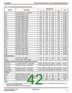
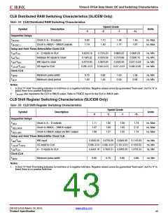
CLB Distributed RAM Switching Characteristics (SLICEM Only)
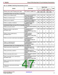
Table 55: CLB Distributed RAM Switching Characteristics
Speed Grade
Symbol
Description
Units
-3
-2
-1
-1L
Sequential Delays
TSHCKO
Clock to A – B outputs
0.92
1.19
1.10
1.40
1.36
1.71
1.49
1.87
ns, Max
ns, Max
TSHCKO_1
Clock to AMUX – BMUX outputs
Setup and Hold Times Before/After Clock CLK
T
DS/TDH
TAS/TAH
WS/TWH
A – D inputs to CLK
Address An inputs to clock
WE input to clock
0.62/0.18
0.19/0.52
0.27/0.00
0.28/–0.01
0.72/0.20
0.22/0.59
0.32/0.00
0.34/–0.01
0.88/0.22
0.27/0.66
0.40/0.00
0.41/–0.01
0.98/0.23
0.30/0.75
0.47/–0.03
0.48/–0.05
ns, Min
ns, Min
ns, Min
ns, Min
T
TCECK/TCKCE
Clock CLK
TMPW
CE input to CLK
Minimum pulse width
Minimum clock period
0.70
1.40
0.82
1.64
1.00
2.00
1.04
2.08
ns, Min
ns, Min
TMCP
Notes:
1. A Zero “0” Hold Time listing indicates no hold time or a negative hold time. Negative values cannot be guaranteed “best-case”, but if a “0” is
listed, there is no positive hold time.
2.
T
also represents the CLK to XMUX output. Refer to TRACE report for the CLK to XMUX path.
SHCKO
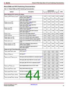
CLB Shift Register Switching Characteristics (SLICEM Only)
Table 56: CLB Shift Register Switching Characteristics
Speed Grade
Symbol
Description
Units
-3
-2
-1
-1L
Sequential Delays
TREG
Clock to A – D outputs
1.11
1.37
1.08
1.30
1.60
1.27
1.58
1.93
1.55
1.74
2.12
1.74
ns, Max
ns, Max
ns, Max
TREG_MUX
TREG_M31
Clock to AMUX – DMUX output
Clock to DMUX output via M31 output
Setup and Hold Times Before/After Clock CLK
T
WS/TWH
TCECK/TCKCE
DS/TDH
WE input
0.05/0.00
0.07/0.00
0.09/0.00
0.11/0.03
ns, Min
ns, Min
ns, Min
CE input to CLK
A – D inputs to CLK
0.06/–0.01 0.08/–0.01 0.10/–0.01 0.12/0.02
T
0.64/0.18
0.60
0.76/0.21
0.70
0.94/0.24
0.85
1.07/0.23
0.89
Clock CLK
TMPW
Minimum pulse width
ns, Min
Notes:
1. A Zero “0” Hold Time listing indicates no hold time or a negative hold time. Negative values cannot be guaranteed “best-case”, but if a “0” is
listed, there is no positive hold time.
DS152 (v3.6) March 18, 2014
www.xilinx.com
Product Specification
43

 XILINX [ XILINX, INC ]