Virtex-6 FPGA Data Sheet: DC and Switching Characteristics
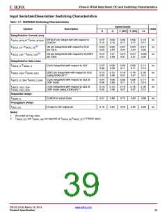
Input Serializer/Deserializer Switching Characteristics
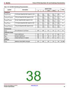
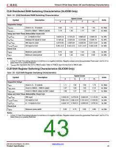
Table 51: ISERDES Switching Characteristics
Speed Grade
Symbol
Description
Units
-3
-2
-1 (XC) -1 (XQ)
-1L
Setup/Hold for Control Lines
TISCCK_BITSLIP/ TISCKC_BITSLIP BITSLIP pin Setup/Hold with respect to
CLKDIV
0.07/
0.15
0.08/
0.16
0.09/
0.17
0.09/
0.17
0.14/
0.17
ns
ns
ns
(2)
TISCCK_CE / TISCKC_CE
CE pin Setup/Hold with respect to CLK
(for CE1)
0.20/
0.03
0.25/
0.04
0.27/
0.04
0.27/
0.04
0.31/
0.05
(2)
T
ISCCK_CE2 / TISCKC_CE2
CE pin Setup/Hold with respect to CLKDIV
(for CE2)
0.01/
0.27
0.01
0.29
0.01/
0.31
0.01/
0.31
–0.05/
0.35
Setup/Hold for Data Lines
TISDCK_D /TISCKD_D
D pin Setup/Hold with respect to CLK
0.07/
0.08
0.08/
0.09
0.09/
0.11
0.09/
0.11
0.11/
0.19
ns
ns
ns
ns
TISDCK_DDLY /TISCKD_DDLY
DDLY pin Setup/Hold with respect to CLK
(using IODELAY)(1)
0.10/
0.05
0.12/
0.06
0.14/
0.07
0.14/
0.07
0.16/
0.15
TISDCK_D_DDR /TISCKD_D_DDR
D pin Setup/Hold with respect to CLK at
DDR mode
0.07/
0.08
0.08/
0.09
0.09/
0.11
0.09/
0.11
0.11/
0.19
TISDCK_DDLY_DDR
TISCKD_DDLY_DDR
D pin Setup/Hold with respect to CLK at
DDR mode (using IODELAY)(1)
0.10/
0.05
0.12/
0.06
0.14/
0.07
0.14/
0.07
0.16/
0.15
Sequential Delays
TISCKO_Q
CLKDIV to out at Q pin
D input to DO output pin
0.57
0.19
0.66
0.22
0.75
0.25
0.80
0.25
0.88
0.28
ns
ns
Propagation Delays
TISDO_DO
Notes:
1. Recorded at 0 tap value.
2.
T
and T
are reported as T
/T
in TRACE report.
ISCCK_CE2
ISCKC_CE2
ISCCK_CE ISCKC_CE
DS152 (v3.6) March 18, 2014
www.xilinx.com
Product Specification
39

 XILINX [ XILINX, INC ]