Virtex-6 FPGA Data Sheet: DC and Switching Characteristics
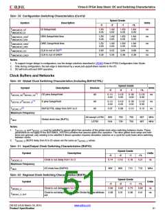
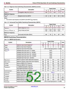
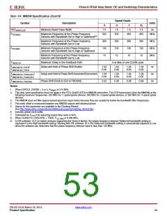
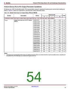
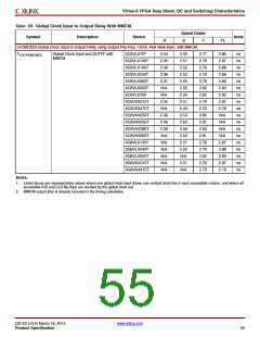
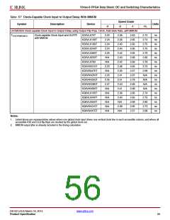
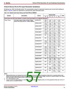
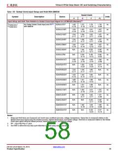
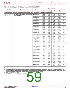
Table 66: Global Clock Input to Output Delay With MMCM
Speed Grade
Symbol
Description
Device
Units
-3
-2
-1
-1L
LVCMOS25 Global Clock Input to Output Delay using Output Flip-Flop, 12mA, Fast Slew Rate, with MMCM.
TICKOFMMCMGC
Global Clock Input and OUTFF with
MMCM
XC6VLX75T
2.34
2.35
2.36
2.36
2.37
N/A
N/A
2.35
N/A
2.36
2.46
2.39
N/A
N/A
N/A
N/A
N/A
N/A
2.50
2.51
2.52
2.52
2.53
2.55
2.54
2.51
2.43
2.53
2.63
2.59
2.54
2.51
2.52
N/A
2.77
2.78
2.79
2.79
2.79
2.82
2.82
2.79
2.70
2.80
2.91
2.83
2.81
2.78
2.79
2.82
2.79
2.70
2.85
2.87
2.88
2.88
2.89
2.93
2.92
2.87
2.79
N/A
ns
ns
ns
ns
ns
ns
ns
ns
ns
ns
ns
ns
ns
ns
ns
ns
ns
ns
XC6VLX130T
XC6VLX195T
XC6VLX240T
XC6VLX365T
XC6VLX550T
XC6VLX760
XC6VSX315T
XC6VSX475T
XC6VHX250T
XC6VHX255T
XC6VHX380T
XC6VHX565T
XQ6VLX130T
XQ6VLX240T
XQ6VLX550T
XQ6VSX315T
XQ6VSX475T
N/A
N/A
N/A
2.87
2.88
2.93
2.87
2.79
2.51
N/A
Notes:
1. Listed above are representative values where one global clock input drives one vertical clock line in each accessible column, and where all
accessible IOB and CLB flip-flops are clocked by the global clock net.
2. MMCM output jitter is already included in the timing calculation.
DS152 (v3.6) March 18, 2014
www.xilinx.com
Product Specification
55

 XILINX [ XILINX, INC ]