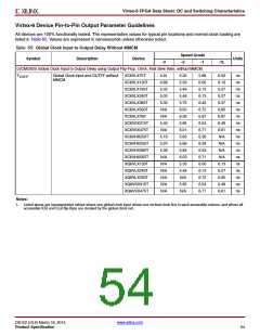
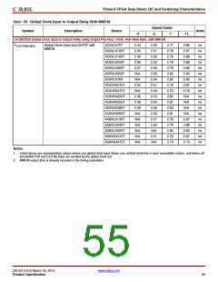
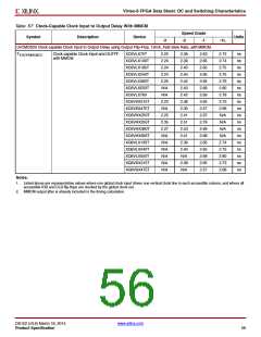
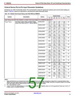
Virtex-6 FPGA Data Sheet: DC and Switching Characteristics
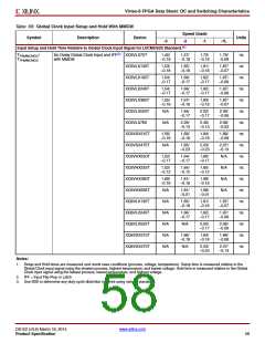
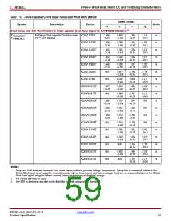
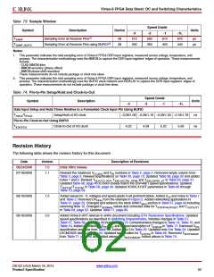
Table 69: Global Clock Input Setup and Hold With MMCM
Speed Grade
Symbol
Description
Device
Units
-3
-2
-1
-1L
Input Setup and Hold Time Relative to Global Clock Input Signal for LVCMOS25 Standard.(1)
TPSMMCMGC
/
No Delay Global Clock Input and IFF(2) XC6VLX75T
with MMCM
1.45/
–0.18
1.57/
–0.18
1.72/
–0.18
1.78/
–0.08
ns
ns
ns
ns
ns
ns
ns
ns
ns
ns
ns
ns
ns
ns
ns
ns
ns
ns
TPHMMCMGC
XC6VLX130T
XC6VLX195T
XC6VLX240T
XC6VLX365T
XC6VLX550T
XC6VLX760
1.53/
–0.18
1.65/
–0.18
1.81/
–0.18
1.87/
–0.07
1.54/
–0.17
1.66/
–0.17
1.82/
–0.17
1.87/
–0.08
1.54/
–0.17
1.66/
–0.17
1.82/
–0.17
1.87/
–0.08
1.55/
–0.18
1.67/
–0.18
1.83/
–0.18
1.87/
–0.07
N/A
1.84/
–0.17
2.02/
–0.17
2.06/
–0.06
N/A
2.26/
–0.13
2.49/
–0.13
2.06/
–0.03
XC6VSX315T
XC6VSX475T
XC6VHX250T
XC6VHX255T
XC6VHX380T
XC6VHX565T
XQ6VLX130T
XQ6VLX240T
XQ6VLX550T
XQ6VSX315T
XQ6VSX475T
1.56/
–0.18
1.68/
–0.18
1.84/
–0.18
1.89/
–0.08
N/A
1.85/
–0.23
2.03/
–0.23
2.07/
–0.13
1.52/
–0.17
1.64/
–0.17
1.80/
–0.17
N/A
N/A
N/A
N/A
1.52/
–0.12
1.64/
–0.12
1.85/
–0.12
1.68/
–0.16
1.81/
–0.16
1.99/
–0.16
N/A
N/A
N/A
N/A
N/A
N/A
1.81/
–0.01
1.99/
–0.01
1.65/
–0.18
1.81/
–0.18
1.87/
–0.07
1.66/
–0.17
1.82/
–0.17
1.87/
–0.08
N/A
2.02/
–0.17
2.06/
–0.06
1.68/
–0.18
1.84/
–0.18
1.89/
–0.08
N/A
2.03/
2.07/
–0.23
–0.13
Notes:
1. Setup and Hold times are measured over worst case conditions (process, voltage, temperature). Setup time is measured relative to the
Global Clock input signal using the slowest process, highest temperature, and lowest voltage. Hold time is measured relative to the Global
Clock input signal using the fastest process, lowest temperature, and highest voltage.
2. IFF = Input Flip-Flop or Latch
3. Use IBIS to determine any duty-cycle distortion incurred using various standards.
DS152 (v3.6) March 18, 2014
www.xilinx.com
Product Specification
58

 XILINX [ XILINX, INC ]