Virtex-6 FPGA Data Sheet: DC and Switching Characteristics
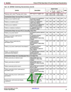
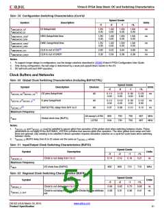
Table 59: Configuration Switching Characteristics (Cont’d)
Symbol Description
Speed Grade
Units
-3
-2
-1
-1L
TMMCMDCK_DI
TMMCMCKD_DI
/
DI Setup/Hold
1.25/
0.00
1.40/
0.00
1.63/
0.00
1.64/
0.00
ns
TMMCMDCK_DEN
/
DEN Setup/Hold time
DWE Setup/Hold time
1.25/
0.00
1.40/
0.00
1.63/
0.00
1.64/
0.00
ns
ns
TMMCMCKD_DEN
TMMCMDCK_DWE
TMMCMCKD_DWE
/
1.25/
0.00
1.40/
0.00
1.63/
0.00
1.64/
0.00
TMMCMCKO_DO
CLK to out of DO(3)
CLK to out of DRDY
2.60
0.32
3.02
0.34
3.64
0.38
3.68
0.38
ns
ns
TMMCMCKO_DRDY
Notes:
1. To support longer delays in configuration, use the design solutions described in UG360:Virtex-6 FPGA Configuration User Guide.
2. Only during configuration, the last edge is determined by a weak pull-up/pull-down resistor in the I/O.
3. DO will hold until next DRP operation.
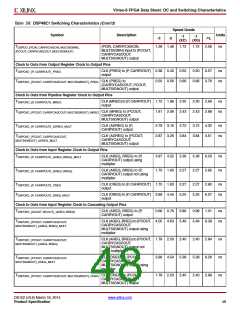
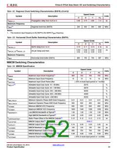
Clock Buffers and Networks
Table 60: Global Clock Switching Characteristics (Including BUFGCTRL)
Speed Grade
Symbol
Description
CE pins Setup/Hold
Devices
Units
-3
-2
-1
-1L
(1)
TBCCCK_CE/TBCCKC_CE
All
0.11/
0.00
0.13/
0.00
0.16/
0.00
0.13/
0.00
ns
(1)
TBCCCK_S/TBCCKC_S
S pins Setup/Hold
All
All
0.11/
0.00
0.13/
0.00
0.16/
0.00
0.13/
0.00
ns
ns
(2)
TBCCKO_O
BUFGCTRL delay from I0/I1 to O
0.07
0.08
0.10
0.10
Maximum Frequency
All except LX760
LX760
800
N/A
750
700
700
700
667
667
MHz
MHz
FMAX
Global clock tree (BUFG)
Notes:
1.
T
and T
must be satisfied to assure glitch-free operation of the global clock when switching between clocks. These
BCCCK_CE
BCCKC_CE
parameters do not apply to the BUFGMUX_VIRTEX4 primitive that assures glitch-free operation. The other global clock setup and hold
times are optional; only needing to be satisfied if device operation requires simulation matches on a cycle-for-cycle basis when switching
between clocks.
2.
T
(BUFG delay from I0 to O) values are the same as T
values.
BCCKO_O
BGCKO_O
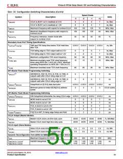
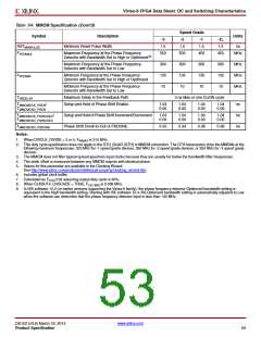
Table 61: Input/Output Clock Switching Characteristics (BUFIO)
Symbol Description
TBIOCKO_O Clock to out delay from I to O
Speed Grade
Units
-3
-2
-1
-1L
0.14
0.16
0.18
0.21
ns
Maximum Frequency
FMAX
I/O clock tree (BUFIO)
800
800
710
710
MHz
Table 62: Regional Clock Switching Characteristics (BUFR)
Symbol Description
Clock to out delay from I to O
Speed Grade
Units
-3
-2
-1
-1L
0.82
0.41
TBRCKO_O
0.56
0.28
0.62
0.31
0.73
0.36
ns
ns
Clock to out delay from I to O with Divide Bypass attribute
set
TBRCKO_O_BYP
DS152 (v3.6) March 18, 2014
www.xilinx.com
Product Specification
51

 XILINX [ XILINX, INC ]