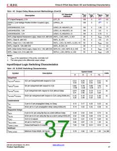
Virtex-6 FPGA Data Sheet: DC and Switching Characteristics
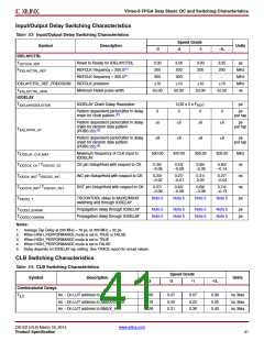
Input/Output Delay Switching Characteristics
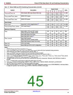
Table 53: Input/Output Delay Switching Characteristics
Speed Grade
Symbol
Description
Units
-3
-2
-1
-1L
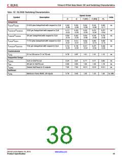
IDELAYCTRL
TDLYCCO_RDY
Reset to Ready for IDELAYCTRL
REFCLK frequency = 200.0(1)
REFCLK frequency = 300.0(1)
REFCLK precision
3.00
200
3.00
200
3.00
200
–
3.25
200
–
µs
FIDELAYCTRL_REF
MHz
MHz
MHz
ns
300
300
IDELAYCTRL_REF_PRECISION
TIDELAYCTRL_RPW
10
10
10
10
Minimum Reset pulse width
50.00
50.00
50.00
52.50
IODELAY
TIDELAYRESOLUTION
IODELAY Chain Delay Resolution
1/(32 x 2 x FREF
)
ps
Pattern dependent period jitter in delay
chain for clock pattern.(2)
0
5
0
0
0
5
ps
per tap
Pattern dependent period jitter in delay
chain for random data pattern
(PRBS 23).(3)
5
5
ps
per tap
TIDELAYPAT_JIT
Pattern dependent period jitter in delay
chain for random data pattern
(PRBS 23).(4)
9
9
9
9
ps
per tap
TIODELAY_CLK_MAX
Maximum frequency of CLK input to
IODELAY
500.00
420.00
300.00
300.00
MHz
ns
TIODCCK_CE / TIODCKC_CE
CE pin Setup/Hold with respect to CK
INC pin Setup/Hold with respect to CK
RST pin Setup/Hold with respect to CK
0.45/
–0.09
0.53/
–0.09
0.65/
–0.09
0.84/
–0.14
T
IODCK_INC/ TIODCKC_INC
TIODCCK_RST/ TIODCKC_RST
TIODDO_T
0.23/
–0.02
0.27/
–0.01
0.31/
0.00
0.27/
–0.04
ns
0.57/
–0.08
0.62/
–0.08
0.69/
–0.08
0.74/
–0.13
ns
TSCONTROL delay to MUXE/MUXF
switching and through IODELAY
Note 5
Note 5
Note 5
Note 5
ps
TIODDO_IDATAIN
TIODDO_ODATAIN
Propagation delay through IODELAY
Propagation delay through IODELAY
Note 5
Note 5
Note 5
Note 5
Note 5
Note 5
Note 5
Note 5
ps
ps
Notes:
1. Average Tap Delay at 200 MHz = 78 ps, at 300 MHz = 52 ps.
2. When HIGH_PERFORMANCE mode is set to TRUE or FALSE.
3. When HIGH_PERFORMANCE mode is set to TRUE
4. When HIGH_PERFORMANCE mode is set to FALSE.
5. Delay depends on IODELAY tap setting. See TRACE report for actual values.
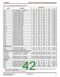
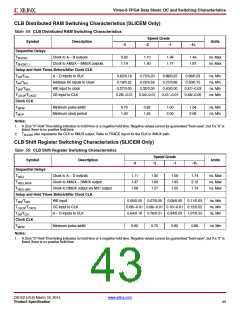
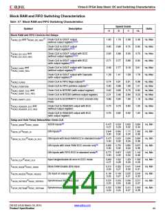
CLB Switching Characteristics
Table 54: CLB Switching Characteristics
Speed Grade
Symbol
Description
Units
-3
-2
-1
-1L
Combinatorial Delays
TILO
An – Dn LUT address to A
0.06
0.18
0.28
0.07
0.20
0.31
0.07
0.22
0.36
0.09
0.25
0.40
ns, Max
ns, Max
ns, Max
An – Dn LUT address to AMUX/CMUX
An – Dn LUT address to BMUX_A
DS152 (v3.6) March 18, 2014
www.xilinx.com
Product Specification
41

 XILINX [ XILINX, INC ]