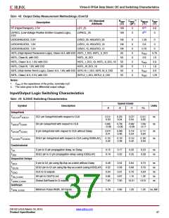
Virtex-6 FPGA Data Sheet: DC and Switching Characteristics
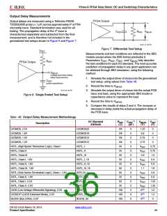
Table 48: Output Delay Measurement Methodology (Cont’d)
(1)
I/O Standard
Attribute
RREF CREF
VMEAS VREF
Description
HT (HyperTransport), 2.5V
(Ω)
100
100
(pF)
(V)
0(2)
0(2)
(V)
0.6
0
LDT_25
0
0
LVPECL (Low-Voltage Positive Emitter-Coupled Logic),
2.5V
LVPECL_25
LVDCI/HSLVDCI, 2.5V
LVDCI/HSLVDCI, 1.8V
LVDCI/HSLVDCI, 1.5V
LVDCI_25, HSLVDCI_25
LVDCI_18, HSLVDCI_18
LVDCI_15, HSLVDCI_15
1M
1M
1M
50
50
50
50
50
50
0
0
0
0
0
0
0
0
0
1.25
0.9
0
0
0.75
VREF
0.9
0
HSTL (High-Speed Transceiver Logic), Class I & II, with DCI HSTL_I_DCI, HSTL_II_DCI
0.75
1.5
0.9
1.8
0.9
1.25
HSTL, Class III, with DCI
HSTL_III_DCI
HSTL, Class I & II, 1.8V, with DCI
HSTL, Class III, 1.8V, with DCI
HSTL_I_DCI_18, HSTL_II_DCI_18
HSTL_III_DCI_18
VREF
1.1
SSTL (Stub Series Termi.Logic), Class I & II, 1.8V, with DCI SSTL18_I_DCI, SSTL18_II_DCI
VREF
VREF
SSTL, Class I & II, 2.5V, with DCI
SSTL2_I_DCI, SSTL2_II_DCI
Notes:
1.
C
is the capacitance of the probe, nominally 0 pF.
REF
2. The value given is the differential output voltage.
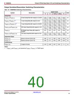
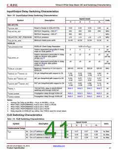
Input/Output Logic Switching Characteristics
Table 49: ILOGIC Switching Characteristics
Speed Grade
Symbol
Description
Units
-3
-2
-1
-1L
Setup/Hold
TICE1CK/TICKCE1
TISRCK/TICKSR
TIDOCK/TIOCKD
CE1 pin Setup/Hold with respect to CLK
0.21/
0.03
0.25/
0.04
0.27/
0.04
0.31/
0.05
ns
ns
ns
ns
SR pin Setup/Hold with respect to CLK
0.66/
–0.08
0.78/
–0.08
0.96/
–0.08
1.09/
–0.11
D pin Setup/Hold with respect to CLK without Delay
DDLY pin Setup/Hold with respect to CLK (using IODELAY)
0.07/
0.41
0.08/
0.46
0.10/
0.54
0.11/
0.64
T
IDOCKD/TIOCKDD
0.10/
0.32
0.12/
0.36
0.14/
0.42
0.16/
0.50
Combinatorial
TIDI
D pin to O pin propagation delay, no Delay
0.15
0.19
0.17
0.22
0.20
0.25
0.23
0.28
ns
ns
TIDID
DDLY pin to O pin propagation delay (using IODELAY)
Sequential Delays
TIDLO
D pin to Q1 pin using flip-flop as a latch without Delay
DDLY pin to Q1 pin using flip-flop as a latch (using IODELAY)
CLK to Q outputs
0.48
0.52
0.54
0.85
7.60
0.54
0.58
0.61
0.97
7.60
0.64
0.68
0.70
1.15
10.51
0.73
0.78
0.93
1.32
10.51
ns
ns
ns
ns
ns
TIDLOD
TICKQ
TRQ_ILOGIC
TGSRQ_ILOGIC
Set/Reset
TRPW_ILOGIC
SR pin to OQ/TQ out
Global Set/Reset to Q outputs
Minimum Pulse Width, SR inputs
0.78
0.95
1.20
1.30
ns, Min
DS152 (v3.6) March 18, 2014
www.xilinx.com
Product Specification
37

 XILINX [ XILINX, INC ]