Virtex-6 FPGA Data Sheet: DC and Switching Characteristics
Block RAM and FIFO Switching Characteristics
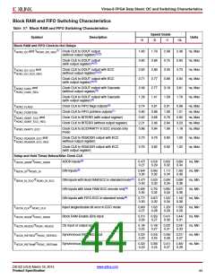
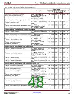
Table 57: Block RAM and FIFO Switching Characteristics
Speed Grade
Symbol
Description
Units
-3
-2
-1
-1L
Block RAM and FIFO Clock-to-Out Delays
(1)
TRCKO_DO and TRCKO_DO_REG
Clock CLK to DOUT output
(without output register)(2)(3)
1.60
0.60
2.62
0.71
2.49
1.29
1.79
0.66
2.89
0.77
2.77
1.41
2.08
0.75
3.30
0.86
3.18
1.58
2.36
0.83
3.73
0.94
3.61
1.79
ns, Max
ns, Max
ns, Max
ns, Max
ns, Max
ns, Max
Clock CLK to DOUT output
(with output register)(4)(5)
T
RCKO_DO_ECC and
Clock CLK to DOUT output with ECC
(without output register)(2)(3)
TRCKO_DO_ECC_REG
Clock CLK to DOUT output with ECC
(with output register)(4)(5)
TRCKO_CASC and
TRCKO_CASC_REG
Clock CLK to DOUT output with Cascade
(without output register)(2)
Clock CLK to DOUT output with Cascade
(with output register)(4)
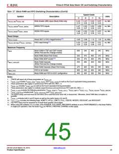
TRCKO_FLAGS
Clock CLK to FIFO flags outputs(6)
0.74
0.90
0.62
2.21
0.86
0.81
0.98
0.68
2.46
0.94
0.91
1.09
0.76
2.84
1.06
0.98
1.21
0.82
3.23
1.18
ns, Max
ns, Max
ns, Max
ns, Max
ns, Max
TRCKO_POINTERS
Clock CLK to FIFO pointers outputs(7)
Clock CLK to BITERR (with output register)
Clock CLK to BITERR (without output register)
T
RCKO_SDBIT_ECC and
TRCKO_SDBIT_ECC_REG
TRCKO_PARITY_ECC
Clock CLK to ECCPARITY in ECC encode only
mode
TRCKO_RDADDR_ECC and
TRCKO_RDADDR_ECC_REG
Clock CLK to RDADDR output with ECC
(without output register)
0.73
0.76
0.79
0.82
0.90
0.92
1.00
1.02
ns, Max
ns, Max
Clock CLK to RDADDR output with ECC
(with output register)
Setup and Hold Times Before/After Clock CLK
T
RCCK_ADDR/TRCKC_ADDR
ADDR inputs(8)
0.47/
0.27
0.53/
0.29
0.62/
0.32
0.66/
0.34
ns, Min
ns, Min
ns, Min
ns, Min
ns, Min
ns, Min
ns, Min
ns, Min
ns, Min
ns, Min
T
RDCK_DI/TRCKD_DI
DIN inputs(9)
0.84/
0.30
0.95/
0.32
1.11/
0.34
1.26/
0.36
TRDCK_DI_ECC/TRCKD_DI_ECC
DIN inputs with block RAM ECC in standard mode(9) 0.47/
0.30
0.52/
0.32
0.59/
0.34
0.68/
0.36
DIN inputs with block RAM ECC encode only(9)
DIN inputs with FIFO ECC in standard mode(9)
Inject single/double bit error in ECC mode
Block RAM Enable (EN) input
0.68/
0.30
0.75/
0.32
0.85/
0.34
0.97/
0.36
0.77/
0.30
0.87/
0.32
1.02/
0.34
1.16/
0.36
TRCCK_CLK/TRCKC_CLK
0.90/
0.27
1.02/
0.28
1.20/
0.29
1.56/
0.29
TRCCK_RDEN/TRCKC_RDEN
0.31/
0.26
0.35/
0.27
0.41/
0.30
0.44/
0.31
T
RCCK_REGCE/TRCKC_REGCE
TRCCK_RSTREG/TRCKC_RSTREG
RCCK_RSTRAM/TRCKC_RSTRAM
CE input of output register
0.18/
0.25
0.19/
0.27
0.22/
0.31
0.24/
0.33
Synchronous RSTREG input
0.22/
0.23
0.24/
0.24
0.28/
0.26
0.31/
0.27
T
Synchronous RSTRAM input
0.32/
0.23
0.36/
0.24
0.41/
0.27
0.46/
0.29
DS152 (v3.6) March 18, 2014
www.xilinx.com
Product Specification
44

 XILINX [ XILINX, INC ]