Virtex-6 FPGA Data Sheet: DC and Switching Characteristics
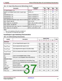
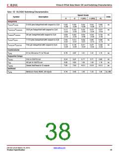
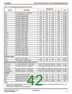
Table 50: OLOGIC Switching Characteristics
Speed Grade
Units
Symbol
Description
-3
-2
-1 (XC)
-1 (XQ)
-1L
Setup/Hold
TODCK/TOCKD
D1/D2 pins Setup/Hold with respect to CLK
OCE pin Setup/Hold with respect to CLK
SR pin Setup/Hold with respect to CLK
T1/T2 pins Setup/Hold with respect to CLK
TCE pin Setup/Hold with respect to CLK
0.45/
–0.08
0.50/
–0.08
0.54/
–0.08
0.54/
–0.08
0.69/
–0.11
ns
ns
ns
ns
ns
TOOCECK/TOCKOCE
0.17/
–0.03
0.20/
–0.03
0.22/
–0.03
0.27/
–0.05
0.27/
–0.04
TOSRCK/TOCKSR
0.59/
–0.24
0.62/
–0.24
0.54/
–0.08
0.54/
–0.08
0.79/
–0.35
TOTCK/TOCKT
0.44/
–0.07
0.51/
–0.07
0.56/
–0.07
0.60/
–0.10
0.68/
–0.13
TOTCECK/TOCKTCE
0.15/
–0.04
0.19/
–0.04
0.21/
–0.04
0.27/
–0.05
0.29/
–0.05
Combinatorial
TDOQ
D1 to OQ out or T1 to TQ out
0.78
0.87
1.01
1.01
1.15
ns
Sequential Delays
TOCKQ
CLK to OQ/TQ out
0.54
0.80
7.60
0.61
0.90
7.60
0.71
1.05
0.71
1.05
0.80
1.19
ns
ns
ns
TRQ
SR pin to OQ/TQ out
TGSRQ
Global Set/Reset to Q outputs
10.51
10.51
10.51
Set/Reset
TRPW
Minimum Pulse Width, SR inputs
0.78
0.95
1.20
1.20
1.30
ns, Min
DS152 (v3.6) March 18, 2014
www.xilinx.com
Product Specification
38

 XILINX [ XILINX, INC ]