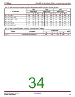
Virtex-6 FPGA Data Sheet: DC and Switching Characteristics
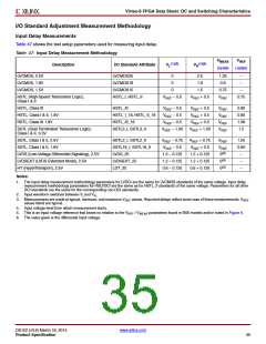
Output Delay Measurements
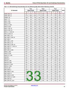
X-Ref Target - Figure 7
FPGA Output
Output delays are measured using a Tektronix P6245
TDS500/600 probe (< 1 pF) across approximately 4" of FR4
microstrip trace. Standard termination was used for all
testing. The propagation delay of the 4" trace is
+
CREF
RREF VMEAS
characterized separately and subtracted from the final
measurement, and is therefore not included in the
generalized test setups shown in Figure 6 and Figure 7.
–
ds152_07_042109
X-Ref Target - Figure 6
Figure 7: Differential Test Setup
VREF
Measurements and test conditions are reflected in the IBIS
models except where the IBIS format precludes it.
Parameters V
, R
, C
, and V
fully describe
REF
REF
REF
MEAS
RREF
FPGA Output
the test conditions for each I/O standard. The most accurate
prediction of propagation delay in any given application can
be obtained through IBIS simulation, using the following
method:
VMEAS
(voltage level when taking
delay measurement)
1. Simulate the output driver of choice into the generalized
test setup, using values from Table 48.
CREF
(probe capacitance)
2. Record the time to V
.
MEAS
ds152_06_042109
3. Simulate the output driver of choice into the actual PCB
trace and load, using the appropriate IBIS model or
capacitance value to represent the load.
Figure 6: Single Ended Test Setup
4. Record the time to V
.
MEAS
5. Compare the results of steps 2 and 4. The increase or
decrease in delay yields the actual propagation delay of
the PCB trace.
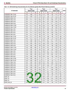
Table 48: Output Delay Measurement Methodology
(1)
I/O Standard
Attribute
RREF CREF
VMEAS VREF
Description
(Ω)
1M
1M
1M
1M
50
(pF)
0
(V)
1.25
0.9
(V)
LVCMOS, 2.5V
LVCMOS25
0
LVCMOS, 1.8V
LVCMOS18
LVCMOS15
LVCMOS12
HSTL_I
0
0
LVCMOS, 1.5V
0
0.75
0.75
VREF
VREF
0.9
0
LVCMOS, 1.2V
0
0
HSTL (High-Speed Transceiver Logic), Class I
HSTL, Class II
0
0.75
0.75
1.5
0.9
0.9
1.8
0.9
0.9
1.25
1.25
1.2
1.2
0
HSTL_II
25
0
HSTL, Class III
HSTL_III
50
0
HSTL, Class I, 1.8V
HSTL_I_18
HSTL_II_18
HSTL_III_18
SSTL18_I
SSTL18_II
SSTL2_I
50
0
VREF
VREF
1.1
HSTL, Class II, 1.8V
25
0
HSTL, Class III, 1.8V
50
0
SSTL (Stub Series Terminated Logic), Class I, 1.8V
SSTL, Class II, 1.8V
50
0
VREF
VREF
VREF
VREF
0(2)
25
0
SSTL, Class I, 2.5V
50
0
SSTL, Class II, 2.5V
SSTL2_II
LVDS_25
LVDS_25
BLVDS_25
25
0
LVDS (Low-Voltage Differential Signaling), 2.5V
LVDSEXT (LVDS Extended Mode), 2.5V
BLVDS (Bus LVDS), 2.5V
100
100
100
0
0
0(2)
0
0(2)
DS152 (v3.6) March 18, 2014
www.xilinx.com
Product Specification
36

 XILINX [ XILINX, INC ]