Spartan-3E FPGA Family: Pinout Descriptions
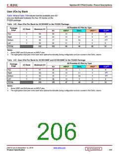
User I/Os by Bank
Table 148 and Table 149 indicate how the available user-I/O
pins are distributed between the four I/O banks on the
FG320 package.
Table 148: User I/Os Per Bank for XC3S500E in the FG320 Package
All Possible I/O Pins by Type
Package
I/O Bank
Maximum I/O
Edge
(2)
I/O
29
INPUT
14
DUAL
1
VREF(1)
CLK
8
Top
0
1
2
3
58
58
6
5
Right
22
10
21
24
0
0(2)
0(2)
8
Bottom
Left
58
17
13
4
58
34
11
5
TOTAL
232
102
48
46
20
16
Notes:
1. Some VREF and CLK pins are on INPUT pins.
2. The eight global clock pins in this bank have optional functionality during configuration and are counted in the DUAL column.
Table 149: User I/Os Per Bank for XC3S1200E and XC3S1600E in the FG320 Package
All Possible I/O Pins by Type
Package
I/O Bank
Maximum I/O
Edge
(2)
I/O
INPUT
DUAL
VREF(1)
CLK
8
Top
0
1
2
3
61
63
34
12
1
6
5
Right
25
12
21
24
0
0(2)
0(2)
8
Bottom
Left
63
23
11
5
63
38
12
5
TOTAL
250
120
47
46
21
16
Notes:
1. Some VREF and CLK pins are on INPUT pins.
2. The eight global clock pins in this bank have optional functionality during configuration and are counted in the DUAL column.
DS312 (v4.2) December 14, 2018
www.xilinx.com
Product Specification
206

 XILINX [ XILINX, INC ]