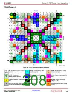
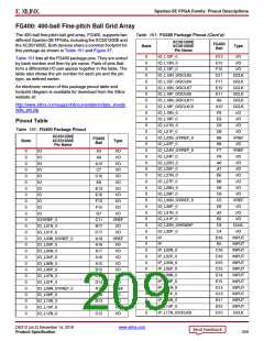
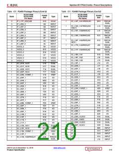
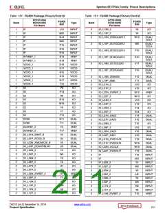
Spartan-3E FPGA Family: Pinout Descriptions
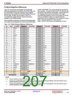
Footprint Migration Differences
Table 150 summarizes any footprint and functionality
differences between the XC3S500E, the XC3S1200E, and
the XC3S1600E FPGAs that may affect easy migration
between devices available in the FG320 package. There are
26 such balls. All other pins not listed in Table 150
unconditionally migrate between Spartan-3E devices
available in the FG320 package.
and the XC3S1600E. The arrows indicate the direction for
easy migration. A double-ended arrow () indicates that
the two pins have identical functionality. A left-facing arrow
() indicates that the pin on the device on the right
unconditionally migrates to the pin on the device on the left.
It may be possible to migrate the opposite direction
depending on the I/O configuration. For example, an I/O pin
(Type = I/O) can migrate to an input-only pin
The XC3S500E is duplicated on both the left and right sides
of the table to show migrations to and from the XC3S1200E
(Type = INPUT) if the I/O pin is configured as an input.
Table 150: FG320 Footprint Migration Differences
Pin
A7
Bank
0
XC3S500E
INPUT
N.C.
Migration
XC3S1200E
I/O
Migration
0
XC3S1600E
I/O
Migration
XC3S500E
INPUT
A12
D4
0
I/O
I/O
N.C.
N.C.
N.C.
INPUT
N.C.
N.C.
N.C.
N.C.
N.C.
I/O
3
N.C.
I/O
I/O
D6
0
N.C.
I/O
I/O
D13
E3
0
INPUT
N.C.
I/O
I/O
3
I/O
I/O
E4
3
N.C.
I/O
I/O
E6
0
N.C.
I/O
I/O
E15
E16
E17
F4
1
N.C.
I/O
I/O
1
N.C.
I/O
I/O
1
I/O
INPUT
INPUT
I/O
INPUT
INPUT
I/O
3
I/O
I/O
N12
N14
N15
P3
2
N.C.
N.C.
N.C.
N.C.
N.C.
N.C.
N.C.
I/O
1
N.C.
I/O
I/O
1
N.C.
I/O
I/O
3
N.C.
I/O
I/O
P4
3
N.C.
I/O
I/O
P12
P15
P16
R4
2
N.C.
I/O
I/O
1
I/O
INPUT
I/O
INPUT
I/O
1
N.C.
N.C.
VREF(I/O)
INPUT
INPUT
N.C.
N.C.
N.C.
3
VREF(I/O)
INPUT
INPUT
N.C.
VREF(INPUT)
I/O
VREF(INPUT)
I/O
U6
2
U13
V5
2
I/O
I/O
2
I/O
I/O
V6
2
N.C.
VREF
I/O
VREF
I/O
V7
2
N.C.
DIFFERENCES
26
26
Legend:
This pin is identical on the device on the left and the right.
This pin can unconditionally migrate from the device on the left to the device on the right. Migration in the other direction may be
possible depending on how the pin is configured for the device on the right.
This pin can unconditionally migrate from the device on the right to the device on the left. Migration in the other direction may be
possible depending on how the pin is configured for the device on the left.
DS312 (v4.2) December 14, 2018
www.xilinx.com
Product Specification
207

 XILINX [ XILINX, INC ]