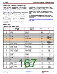
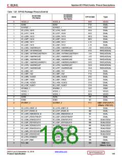
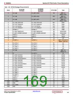
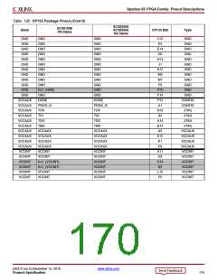
Spartan-3E FPGA Family: Pinout Descriptions
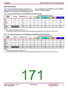
User I/Os by Bank
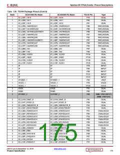
Table 133 shows how the 83 available user-I/O pins are
distributed on the XC3S100E FPGA packaged in the CP132
package. Table 134 indicates how the 92 available user-I/O
pins are distributed on the XC3S250E and the XC3S500E
FPGAs in the CP132 package.
Table 133: User I/Os Per Bank for the XC3S100E in the CP132 Package
All Possible I/O Pins by Type
Package
Edge
I/O Bank
Maximum I/O
(2)
I/O
6
INPUT
DUAL
1
VREF(1)
CLK
Top
0
1
2
3
18
23
22
20
83
2
0
0
0
2
1
2
2
2
7
8
(2)
Right
0
21
20
0
0
0
(2)
Bottom
Left
0
10
16
8
TOTAL
42
16
Notes:
1. Some VREF and CLK pins are on INPUT pins.
2. The eight global clock pins in this bank have optional functionality during configuration and are counted in the DUAL column.
Table 134: User I/Os Per Bank for the XC3S250E and XC3S500E in the CP132 Package
All Possible I/O Pins by Type
Package
I/O Bank
Maximum I/O
Edge
(2)
I/O
11
0
INPUT
DUAL
VREF(1)
CLK
Top
0
1
2
3
22
23
26
21
92
0
0
0
0
0
1
2
2
2
2
8
8
Right
21
24
0
0(2)
0(2)
8
Bottom
Left
0
11
22
TOTAL
46
16
Notes:
1. Some VREF and CLK pins are on INPUT pins.
2. The eight global clock pins in this bank have optional functionality during configuration and are counted in the DUAL column.
DS312 (v4.2) December 14, 2018
www.xilinx.com
Product Specification
171

 XILINX [ XILINX, INC ]