Spartan-3E FPGA Family: Pinout Descriptions
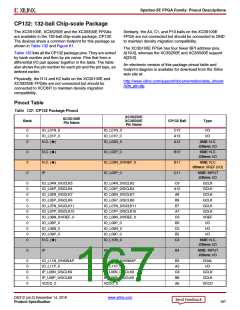
CP132: 132-ball Chip-scale Package
The XC3S100E, XC3S250E and the XC3S500E FPGAs
are available in the 132-ball chip-scale package, CP132.
The devices share a common footprint for this package as
shown in Table 132 and Figure 81.
Similarly, the A4, C1, and P10 balls on the XC3S100E
FPGA are not connected but should be connected to GND
to maintain density migration compatibility.
The XC3S100E FPGA has four fewer BPI address pins,
A[19:0], whereas the XC3S250E and XC3S500E support
A[23:0].
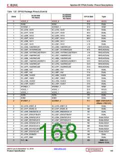
Table 132 lists all the CP132 package pins. They are sorted
by bank number and then by pin name. Pins that form a
differential I/O pair appear together in the table. The table
also shows the pin number for each pin and the pin type, as
defined earlier.
An electronic version of this package pinout table and
footprint diagram is available for download from the Xilinx
web site at:
Physically, the D14 and K2 balls on the XC3S100E and
XC3S250E FPGAs are not connected but should be
connected to VCCINT to maintain density migration
compatibility.
http://www.xilinx.com/support/documentation/data_sheets
/s3e_pin.zip
Pinout Table
Table 132: CP132 Package Pinout
XC3S250E
XC3S500E
Pin Name
XC3S100E
Pin Name
Bank
CP132 Ball
Type
0
0
0
IO_L01N_0
IO_L01P_0
N.C. ()
IO_L01N_0
IO_L01P_0
IO_L02N_0
C12
A13
A12
I/O
I/O
100E: N.C.
Others: I/O
0
0
0
N.C. ()
N.C. ()
IP
IO_L02P_0
B12
B11
C11
100E: N.C.
Others: I/O
IO_L03N_0/VREF_0
IO_L03P_0
100E: N.C.
Others: VREF (I/O)
100E: INPUT
Others: I/O
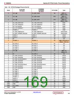
0
0
0
0
0
0
0
0
0
0
0
IO_L04N_0/GCLK5
IO_L04P_0/GCLK4
IO_L05N_0/GCLK7
IO_L05P_0/GCLK6
IO_L07N_0/GCLK11
IO_L07P_0/GCLK10
IO_L08N_0/VREF_0
IO_L08P_0
IO_L04N_0/GCLK5
IO_L04P_0/GCLK4
IO_L05N_0/GCLK7
IO_L05P_0/GCLK6
IO_L07N_0/GCLK11
IO_L07P_0/GCLK10
IO_L08N_0/VREF_0
IO_L08P_0
C9
A10
A9
B9
B7
A7
C6
B6
C5
B5
C4
GCLK
GCLK
GCLK
GCLK
GCLK
GCLK
VREF
I/O
IO_L09N_0
IO_L09N_0
I/O
IO_L09P_0
IO_L09P_0
I/O
N.C. ()
IO_L10N_0
100E: N.C.
Others: I/O
0
IP
IO_L10P_0
B4
100E: INPUT
Others: I/O
0
0
0
0
0
IO_L11N_0/HSWAP
IO_L11P_0
IO_L11N_0/HSWAP
IO_L11P_0
B3
A3
C8
B8
A6
DUAL
I/O
IP_L06N_0/GCLK9
IP_L06P_0/GCLK8
VCCO_0
IP_L06N_0/GCLK9
IP_L06P_0/GCLK8
VCCO_0
GCLK
GCLK
VCCO
DS312 (v4.2) December 14, 2018
www.xilinx.com
Product Specification
167

 XILINX [ XILINX, INC ]