Spartan-3E FPGA Family: Pinout Descriptions
Footprint Migration Differences
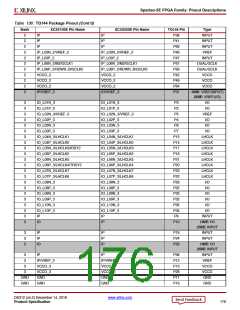
Table 135 summarizes any footprint and functionality
differences between the XC3S100E, the XC3S250E, and
the XC3S500E FPGAs that may affect easy migration
between devices in the CP132 package. There are 14 such
balls. All other pins not listed in Table 135 unconditionally
migrate between Spartan-3E devices available in the
CP132 package.
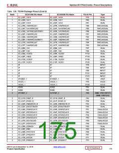
the two pins have identical functionality. A left-facing arrow
() indicates that the pin on the device on the right
unconditionally migrates to the pin on the device on the left.
It may be possible to migrate the opposite direction
depending on the I/O configuration. For example, an I/O pin
(Type = I/O) can migrate to an input-only pin
(Type = INPUT) if the I/O pin is configured as an input.
The XC3S100E is duplicated on both the left and right sides
of the table to show migrations to and from the XC3S250E
and the XC3S500E. The arrows indicate the direction for
easy migration. A double-ended arrow () indicates that
The XC3S100E FPGA in the CP132 package has four fewer
BPI-mode address lines than the XC3S250E and
XC3S500E.
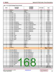
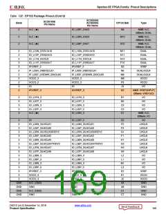
Table 135: CP132 Footprint Migration Differences
CP132
Ball
XC3S100E
Type
XC3S250E
Type
XC3S500E
Type
XC3S100E
Type
Bank
Migration
Migration
Migration
A12
B4
0
0
0
0
0
0
3
3
3
2
2
2
2
2
N.C.
14
I/O
I/O
0
I/O
I/O
14
N.C.
INPUT
N.C.
INPUT
N.C.
B11
B12
C4
I/O
I/O
N.C.
I/O
I/O
N.C.
N.C.
I/O
I/O
N.C.
C11
D1
INPUT
N.C.
I/O
I/O
INPUT
N.C.
I/O
I/O
D2
I/O
I/O (Diff)
VREF(I/O)
DUAL
DUAL
DUAL
DUAL
VREF(I/O)
I/O (Diff)
VREF(I/O)
DUAL
DUAL
DUAL
DUAL
VREF(I/O)
I/O
K3
VREF(INPUT)
N.C.
VREF(INPUT)
N.C.
M9
M10
N9
N.C.
N.C.
N.C.
N.C.
N10
P11
N.C.
N.C.
VREF(INPUT)
VREF(INPUT)
DIFFERENCES
Legend:
This pin is identical on the device on the left and the right.
This pin can unconditionally migrate from the device on the left to the device on the right. Migration in the other direction may be
possible depending on how the pin is configured for the device on the right.
This pin can unconditionally migrate from the device on the right to the device on the left. Migration in the other direction may be
possible depending on how the pin is configured for the device on the left.
DS312 (v4.2) December 14, 2018
www.xilinx.com
Product Specification
172

 XILINX [ XILINX, INC ]