R
XC18V00 Series In-System Programmable Configuration PROMs
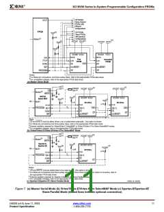
Connecting Configuration PROMs
Connecting the FPGA device with the configuration PROM
(see Figure 5 and Figure 6).
through a user control register in the XC18V00 device. This
control register is accessible through JTAG, and is set using
the “Parallel mode” setting on the Xilinx iMPACT software.
Serial output is the default configuration mode.
•
The DATA output(s) of the PROM(s) drives the D
input of the lead FPGA device.
IN
•
The Master FPGA CCLK output drives the CLK input(s)
of the PROM(s) (in Master-Serial and
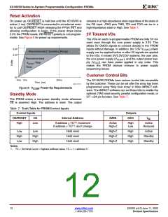
Master Serial Mode Summary
The I/O and logic functions of the Configurable Logic Block
(CLB) and their associated interconnections are estab-
lished by a configuration program. The program is loaded
either automatically upon power up, or on command,
depending on the state of the three FPGA mode pins. In
Master Serial mode, the FPGA automatically loads the con-
figuration program from an external memory. Xilinx PROMs
are designed to accommodate the Master Serial mode.
Master-SelectMAP modes only).
•
•
The CEO output of a PROM drives the CE input of the
next PROM in a daisy chain (if any).
The OE/RESET pins of all PROMs are connected to
the INIT pins of all FPGA devices. This connection
assures that the PROM address counter is reset before
the start of any (re)configuration, even when a
reconfiguration is initiated by a V
glitch.
CCINT
Upon power-up or reconfiguration, an FPGA enters the Mas-
ter Serial mode whenever all three of the FPGA mode-select
pins are Low (M0=0, M1=0, M2=0). Data is read from the
PROM sequentially on a single data line. Synchronization is
provided by the rising edge of the temporary signal CCLK,
which is generated by the FPGA during configuration.
•
•
The PROM CE input can be driven from the DONE pin.
The CE input of the first (or only) PROM can be driven
by the DONE output of all target FPGA devices,
provided that DONE is not permanently grounded. CE
can also be permanently tied Low, but this keeps the
DATA output active and causes an unnecessary supply
current of 10 mA maximum.
Master Serial Mode provides a simple configuration inter-
face. Only a serial data line, a clock line, and two control
lines are required to configure an FPGA. Data from the
PROM is read sequentially, accessed via the internal
address and bit counters which are incremented on every
valid rising edge of CCLK. If the user-programmable,
Slave-Parallel/SelectMap mode is similar to slave serial
mode. The DATA is clocked out of the PROM one byte
per CCLK instead of one bit per CCLK cycle. See FPGA
data sheets for special configuration requirements.
dual-function D pin on the FPGA is used only for configu-
IN
Initiating FPGA Configuration
ration, it must still be held at a defined level during normal
operation. The Xilinx FPGA families take care of this auto-
matically with an on-chip pull-up resistor.
The XC18V00 devices incorporate a pin named CF that is
controllable through the JTAG CONFIG instruction. Execut-
ing the CONFIG instruction through JTAG pulses the CF
low once for 300-500 ns, which resets the FPGA and ini-
tiates configuration.
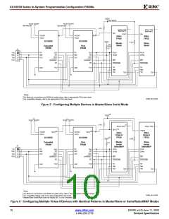
Cascading Configuration PROMs
For multiple FPGAs configured as a serial daisy-chain, or a
single FPGA requiring larger configuration memories in a
serial or SelectMAP configuration mode, cascaded PROMs
provide additional memory (Figure 5). Multiple XC18V00
devices can be concatenated by using the CEO output to
drive the CE input of the downstream device. The clock
inputs and the data outputs of all XC18V00 devices in the
chain are interconnected. After the last data from the first
PROM is read, the next clock signal to the PROM asserts its
CEO output Low and drives its DATA line to a high-imped-
ance state. The second PROM recognizes the Low level on
its CE input and enables its DATA output. See Figure 7.
The CF pin must be connected to the PROGRAM pin on the
FPGA(s) to use this feature.
The iMPACT software can also issue a JTAG CONFIG
command to initiate FPGA configuration through the “Load
FPGA” setting.
The 20-pin packages do not have a dedicated CF pin. For
20-pin packages, the CF --> D4 setting can be used to route
the CF pin function to pin 7 only if the parallel output mode
is not used.
Selecting Configuration Modes
The XC18V00 accommodates serial and parallel methods
of configuration. The configuration modes are selectable
After configuration is complete, address counters of all cas-
caded PROMs are reset if the PROM OE/RESET pin goes
Low or CE goes High.
DS026 (v4.0) June 11, 2003
Product Specification
www.xilinx.com
1-800-255-7778
9

 XILINX [ XILINX, INC ]