R
XC18V00 Series In-System Programmable Configuration PROMs
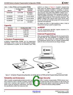
The read security bit can be set by the user to prevent the
internal programming pattern from being read or copied via
JTAG. When set, it allows device erase. Erasing the entire
device is the only way to reset the read security bit.
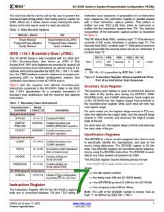
instruction scan sequence. In preparation for an instruction
scan sequence, the instruction register is parallel loaded
with a fixed instruction capture pattern. This pattern is
shifted out onto TDO (LSB first), while an instruction is
shifted into the instruction register from TDI. The detailed
composition of the instruction capture pattern is illustrated
in Figure 3.
Table 3: Data Security Options
Default = Reset
Set
The ISP Status field, IR(4), contains logic “1” if the device is
currently in ISP mode; otherwise, it contains logic “0”. The
Security field, IR(3), contains logic “1” if the device has been
programmed with the security option turned on; otherwise, it
contains logic “0”.
Read Allowed
Program/Erase Allowed
Verify Allowed
Read Inhibited via JTAG
Program/Erase Allowed
Verify Inhibited
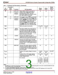
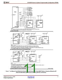
IEEE 1149.1 Boundary-Scan (JTAG)
IR[7:5]
IR[4]
IR[3]
IR[2] IR[1:0]
0 1
The XC18V00 family is fully compliant with the IEEE Std.
1149.1 Boundary-Scan, also known as JTAG. A Test
Access Port (TAP) and registers are provided to support all
required boundary scan instructions, as well as many of the
optional instructions specified by IEEE Std. 1149.1. In addi-
tion, the JTAG interface is used to implement in-system pro-
gramming (ISP) to facilitate configuration, erasure, and
verification operations on the XC18V00 device.
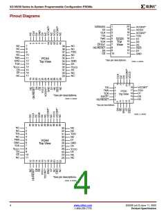
TDI->
0 0 0
ISP
Security
0
->TDO
Status
Notes:
1. IR(1:0) = 01 is specified by IEEE Std. 1149.1
Figure 3: Instruction Register Values Loaded into IR as
Part of an Instruction Scan Sequence
Table 4 lists the required and optional boundary-scan
instructions supported in the XC18V00. Refer to the IEEE
Std. 1149.1 specification for a complete description of
boundary-scan architecture and the required and optional
instructions.
Boundary Scan Register
The boundary-scan register is used to control and observe
the state of the device pins during the EXTEST, SAM-
PLE/PRELOAD, and CLAMP instructions. Each output pin
on the XC18V00 has two register stages that contribute to
the boundary-scan register, while each input pin only has
one register stage.
Table 4: Boundary Scan Instructions
Boundary-Scan
Command
Binary
Code [7:0]
Description
For each output pin, the register stage nearest to TDI con-
trols and observes the output state, and the second stage
closest to TDO controls and observes the High-Z enable
state of the pin.
Required Instructions
BYPASS
11111111 Enables BYPASS
SAMPLE/
PRELOAD
00000001 Enables boundary-scan
SAMPLE/PRELOAD operation
For each input pin, the register stage controls and observes
the input state of the pin.
EXTEST
00000000 Enables boundary-scan
EXTEST operation
Identification Registers
Optional Instructions
The IDCODE is a fixed, vendor-assigned value that is used
to electrically identify the manufacturer and type of the
device being addressed. The IDCODE register is 32 bits
wide. The IDCODE register can be shifted out for examina-
tion by using the IDCODE instruction. The IDCODE is avail-
able to any other system component via JTAG.
CLAMP
11111010 Enables boundary-scan
CLAMP operation
HIGHZ
11111100 all outputs in high-impedance
state simultaneously
IDCODE
11111110 Enables shifting out
32-bit IDCODE
The IDCODE register has the following binary format:
vvvv:ffff:ffff:aaaa:aaaa:cccc:cccc:ccc1
where
USERCODE
11111101 Enables shifting out
32-bit USERCODE
XC18V00 Specific Instructions
v = the die version number
CONFIG
11101110 Initiates FPGA configuration
by pulsing CF pin Low once
f = the family code (50h for XC18V00 family)
a = the ISP PROM product ID (36h for the XC18V04)
c = the company code (49h for Xilinx)
Instruction Register
The Instruction Register (IR) for the XC18V00 is eight bits
wide and is connected between TDI and TDO during an
Note: The LSB of the IDCODE register is always read as
logic “1” as defined by IEEE Std. 1149.1.
DS026 (v4.0) June 11, 2003
Product Specification
www.xilinx.com
1-800-255-7778
7

 XILINX [ XILINX, INC ]